


21555 Non-Transparent PCI-to-PCI Bridge User Manual 93
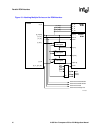
Serial ROM Interface
Prior to a SROM write or write all transaction, the 8-bit write data must be written in the ROM Data CSR.
To initiate the SROM access, the SROM Start bit in the ROM Control CSR is written with a 1 (the PROM Start bit
must be written to a 0 with this access). The 21555 then initiates the SROM access. When the SROM access is
complete, the 21555 automatically clears the SROM Start bit. When the operation is a read, the data then can be
read from the ROM Data register.
The write, write all, erase, and erase all commands may take 10 ms or more to complete, internal to the ROM. A
poll of the SROM must be performed to discover whether these operations are complete. For these commands,
when the SROM access is initiated, the 21555 also sets the SROM_POLL bit in the Table 112, “ROM Control
Register” on page 178. This bit remains asserted after the 21555’s access to the SROM completes. The SROM must
be polled by CSR access and return a ready indication to clear the SROM_POLL bit.
The SROM is polled by the 21555 when the SROM Start bit is written with a 1 when the SROM_POLL bit is set.
The 21555 asserts sr_cs and drives sr_di (pin pr_ad[1]) low. When the SROM drives sr_do (pin pr_ad[2]) high in
response, it has completed the operation internally and the 21555 clears the SROM_POLL bit. The SROM is now
ready for another access.
Note: The SROM_POLL bit must be set for the 21555 to poll the SROM, otherwise the 21555 initiates
another SROM access if the SROM Start bit is written.
A summary of the actions needed for a SROM read access follows:
1. The initiator writes the byte address and the opcode in the ROM Address CSR.
2. The initiator writes the SROM Start bit to a 1 and the PROM Start bit to a 0 in the ROM Control CSR.
3. When the SROM Start bit in the ROM Control CSR is read as a zero, the initiator may read the 8-bit data from
the ROM Data register.
A summary of the actions needed for a write operation follows:
1. The initiator writes the byte address and the opcode in the ROM Address CSR.
2. The initiator writes the 8-bit data in the ROM Data CSR.
3. The initiator writes the SROM Start bit to a 1 and the PROM Start bit to a 0 in the ROM Control CSR in the
same CSR access.
4. When the SROM Start bit in the ROM Control CSR is read as a zero, the initiator polls the SROM to test for
write completion by writing the SROM Start bit to a 1.
5. When the SROM Start bit in the ROM Control CSR is read as a zero, the SROM_POLL bit indicates the status
of the polling operation. When SROM_POLL is read as a one, the SROM should be polled again. When
SROM_POLL is read as a 0, the operation is complete.
The erase, erase all, write enable, and write disable all use write protocol. For all of these operations, however, the
ROM Data register does not need to be written. In addition, the write enable and write disable operations do not
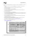
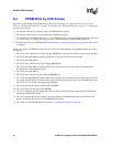
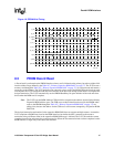
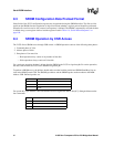
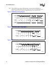
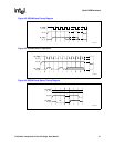
require polling for completion. Figure 19 through Figure 24 show the timing diagrams for SROM read, write, write
all, write enable, write disable, erase, erase all, and check status (polling) operations.