192 21555 Non-Transparent PCI-to-PCI Bridge User Manual
List of Registers
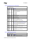
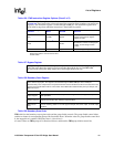
The group disable number column in TBD shows which group disable bit controls the corresponding output driver.
Group disable bits do not affect input-only pins, so those pins have a blank rather than a group number in that
column. The group disable control can control pins on either side of where the group disable boundary-scan register
cell is placed. The group disable boundary-scan register cells have a boundary-scan register order number entry, but
do not have either a corresponding pin number or signal name.
Data shifts from tdi into the most significant bit of the boundary-scan register out to tdo.
Table to be included - TBD.
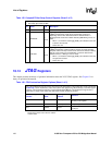
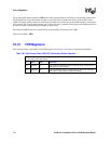
16.15 VPD Registers
This section provides a description of the VPD registers. See Chapter 15 for theory of operation information.
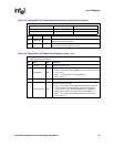
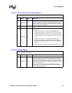
Table 130. Vital Product Data (VPD) ECP ID and Next Pointer Register
• Primary byte offset: E5:E4h
• Secondary byte offset: E5:E4h
Bit Name R/W Description
7:0
VPD ECP
ID
R
VPD Enhanced Capabilities Port ID. Read only as 03h to identify these
ECP registers as VPD registers.
15:8
VPD Next
Ptr
R
Pointer to next ECP registers. Reads as ECh to point to the next set of
ECP registers, supporting CompactPCI Hot
-Swap.


