162 21555 Non-Transparent PCI-to-PCI Bridge User Manual
List of Registers
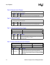
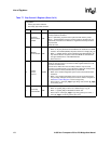
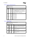
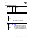
12 I20_ENA R/W
Enables the I20 message unit.
• When 0, the I20 message unit is disabled. Memory accesses to the
Inbound and Outbound FIFO registers at CSR offsets 40h and 44h
result in TRDY# and discarded data on writes, and TRDY# with a
return of FFFFFFFFh on reads.
• When 1, the I20 message unit is enabled. Memory writes cause a
posting to the Inbound Post or Outbound Free list; Reads remove an
entry from the Inbound Free or Outbound Post list.
• Reset value is 0.
15:13 I20_SIZE R/W
Selects the I20 FIFO size. The 21555 supports the following values:
• 000b : 256 entries
• 001b : 512 entries
• 010b : 1 K entries
• 011b : 2 K entries
• 100b : 4 K entries
• 101b : 8 K entries
• 110b : 16 K entries
• 111b : 32 K entries
Reset value is 000b
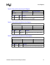
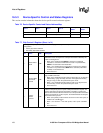
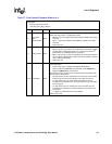
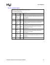
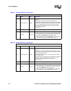
Table 79. Chip Status Register
All of the following conditions can cause the assertion of p_serr_l or s_serr_l if the corresponding SERR#
enable bit is set and the disable bit for this condition is not set.
• Primary byte offset: D1:D0h
• Secondary byte offset: D1:D0h
Bit Name R/W Description
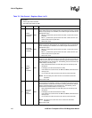
0
Downstream
Delayed
Transaction
Master
Time
-out
R/W1TC
This bit is set to a 1 and p_serr_l is conditionally asserted when the
primary master timeout counter expires and a downstream delayed
transaction completion is discarded from the 21555’s queues.
Reset value is 0
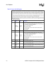
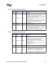
1
Downstream
Delayed
Read
Transaction
Discarded
R/W1TC
This bit is set to a 1 and p_serr_l is conditionally asserted when the
21555 discards a downstream delayed read transaction request after
receiving 2
24
target retries from the secondary bus target (Retry
counters must not be disabled).
Reset value is 0
2
Downstream
Delayed
Write
Transaction
Discarded
R/W1TC
This bit is set to a 1 and p_serr_l is conditionally asserted when the
21555 discards a downstream delayed write transaction request after
receiving 2
24
target retries from the secondary bus target (Retry
counters must not be disabled).
Reset value is 0
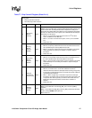
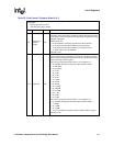
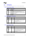
Table 78. Chip Control 1 Register (Sheet 3 of 3)
This register may be preloaded by serial ROM or programmed by the local processor before host
configuration.
• Primary byte offset: CF:CEh
• Secondary byte offset: CF:CEh
Bit Name R/W Description


