188 21555 Non-Transparent PCI-to-PCI Bridge User Manual
List of Registers
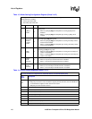
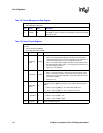
Table 122. Power Management Data Register
• Primary byte offset: E3h
• Secondary byte offset: E3h
Bit Name R/W Description
7:0 PM Data R
Power Management Data register. Reflects one of eight bytes loaded by
serial ROM, or reads as 0. Bytes are selected by the data select register.
Reset value is 00h
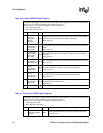
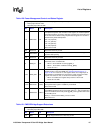
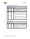
Table 123. Reset Control Register
This register is accessible from the primary interface regardless of the state of the Primary Lockout Reset
Value bit
• Primary byte offset: DB:D8h
• Secondary byte offset: DB:D8h
Bit Name R/W Description
0
Secondary
Reset
R/(WP)
Secondary bus reset.
• When 0, the 21555 deasserts s_rst_l. This bit must be cleared by a
configuration write when it is set by a configuration write. Otherwise, it
clears automatically after 100
µs or when p_rst_l deasserts.
• When 1, the 21555 asserts s_rst_l. This bit is set automatically when
the Chip Reset bit is written with a 1 or when p_rst_l is asserted, or is
set with a configuration write.
• Reset value is 0 (disabled).
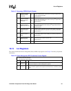
1 Chip Reset R/(WP)
Chip reset control.
• When 1, the 21555 performs a chip reset and to assert s_rst_l. Data
buffers, configuration registers, and both the primary and secondary
interfaces are reset to their initial state. The 21555 clears this bit once
chip reset is complete.
• Reset value is 0
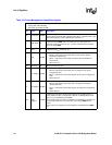
2
Subsystem
Status
R
Reflects the state of the s_pme_l pin. When not used for power
management, the s_pme_l pin may be used to indicate local subsystem
status.
• When 0, signal s_pme_l is at a deasserted high level.
• When 1, signal s_pme_l is at an asserted low level.
3 l_stat Status R
Reflects the state of the l_stat pin.
• When 0, signal l_stat is low.
• When 1, signal l_stat is high.
31:3 Reserved R Reserved. Reads only as 0.


