21555 Non-Transparent PCI-to-PCI Bridge User Manual 81
Parallel ROM Interface 8
This chapter presents the theory of operation information about the 21555 Parallel ROM (PROM) interface. See
Chapter 16 for specific information about the PROM registers.
The 21555 supports the attachment of a standard PROM or EPROM with the addition of a small amount of external
logic. Flash ROMs compatible with Intel’s 28F00x can be used with this interface. The 21555 supports a PCI
expansion ROM BAR on its primary interface with ROM sizes of 4KB to 16MB. Using these features the 21555
can provide the PCI expansion ROM interface for the subsystem. When the local subsystem does not require a PCI
expansion ROM, the expansion ROM BAR can be disabled.
When the host completes the configuration of the primary PCI interface, the PROM may be accessed by the host in
the memory address range assigned by the PCI expansion ROM BAR. The PROM is not directly accessible in the
memory address space of the secondary PCI interface. However, the PROM can be indirectly accessed from both
the primary and secondary PCI interfaces through the 21555 CSRs.
Note: The PROM cannot support simultaneous access using the Table 107, “Primary Expansion ROM
BAR” on page 175 and the Table 112, “ROM Control Register” on page 178 at the same time. The
results are unpredictable. Additionally, the ROM should not be accessed simultaneously from the
primary and secondary interface using the
Table 112, “ROM Control Register” on page 178, otherwise the results are unpredictable.
8.1 Interface Signals
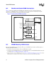
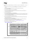
The 21555 expansion ROM interface signals are listed in Table 21. The ROM address is driven out on the 8-bit data
bus in three consecutive cycles. External octal D registers with active low enables are required to capture the ROM
address.
The serial ROM data and clock signals are multiplexed with the ROM signals. A description of the serial ROM
interface is given in Chapter 9. The PROM can also be used to interface other slave-only devices to the ROM address
and data bus. This configuration is described in Section 8.7.


