


21555 Non-Transparent PCI-to-PCI Bridge User Manual 85
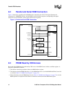
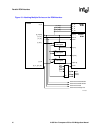
Parallel ROM Interface
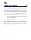
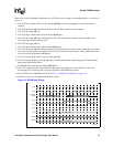
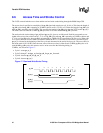
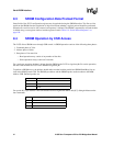
When a byte read of the PROM is performed, the 21555 follows this sequence on the ROM interface, also shown in
Figure 15.
1. The 21555 drives address bits [23:16] on the pr_ad[7:0] pins and asserts pr_ale_l to enable the address
registers.
2. The 21555 drives pr_clk high, latching address bits [23:16] into the first external register.
3. The 21555 drives pr_clk low.
4. The 21555 drives address bits [15:8] on the pr_ad[7:0] pins.
5. The 21555 drives pr_clk high, latching address bits [15:8] into the first external register, and address bits
[23:16] into the second external register.
6. The 21555 drives pr_clk low.
7. The 21555 drives address bits [7:0] on the pr_ad[7:0] pins.
8. The 21555 drives pr_clk high, latching address bits [7:0] into the first external register, address bits [15:8] into
the second external register, and address bits [23:16] into the third external register. All the ROM address bits
are now driven to the appropriate ROM pins.
9. The 21555 deasserts the address register enable, pr_ale_l.
10. The 21555 asserts the pr_cs_l and pr_rd_l pins according to the strobe setup timing specified by the Strobe
Mask in the ROM Setup register.
11. The PROM drives read data onto the pr_ad[7:0] pins.
12. The 21555 samples the read data and deasserts pr_rd_l as specified by the strobe mask. The 21555 also
deasserts pr_cs_l according to the access time specified in the ROM Setup register.
13. The 21555 clears the PROM Start bit in the Table 112, “ROM Control Register” on page 178.
14. Valid data can now be read from the ROM Data register.
.
Figure 15. PROM Read Timing
A7456-01
p_clk
pr_clk
pr_ad[7:0]
d[7:0]
pr_cs_l
pr_rd_l
pr_ale_l
a[7:0]
a[15:8]
a[23:16]
A3 A2
Read Data [7:0]
A1
A3 A2 A1 = Address[7:00]
A3 A2 = Address[15:8]
A3 = Address[23:16]