21555 Non-Transparent PCI-to-PCI Bridge User Manual 147
List of Registers
16.5 PCI Registers
This section covers pages 16-147 through 16-165 and Table 57 through Table 80. See Chapter 3 or Chapter 5 for
theory of operation information.
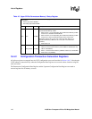
16.5.1 Configuration Registers
The registers described in this section are shared between the primary and secondary interfaces.
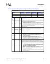
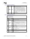
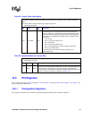
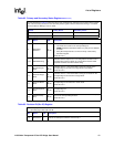
Table 55. Lookup Table Data Register
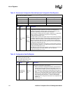
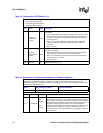
Table 54 and Table 55 are registers that provide a method for the lookup table to be accessed using I/O
transactions, although memory transactions can use either this mechanism or direct access of the lookup
table.
The lookup table is not byte
-writable; byte enables are ignored.
• Byte Offset: 02F:02Ch
Bit Name R/W Description
31:0 LUT_DATA R/W
This register contains the data written to or read from the Lookup Table
at the offset given in the Lookup Table Offset register. When this
register is written, the value written is written to the specified Lookup
Table entry. When this register is read, the value returned reflects the
data read from the specified Lookup Table entry. The following fields
are defined:
• bit 0: valid bit
• bits 2:1: reserved (read only as 0)
• bit 3: prefetchable
• bits 7:4: reserved (read only as 0)
• bits 17:8: translated base or reserved (based on page size)
• bits 31:18: translated base
The lookup table is not reset and therefore powers up to an
indeterminate value.
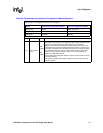
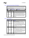
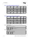
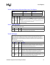
Table 56. Upstream Memory 2 Lookup Table
The lookup table is not byte-writable; byte enables are ignored.
• Byte Offsets: 1FF:100h
Bit Name R/W Description
M2LUT R/W
Contains the lookup table for the Upstream Memory 2 Base Address range.
Each entry in the lookup table is 4 bytes wide. The top 16 to 24 bits, depending
on the page size, of each entry are used to replace the page address of
upstream memory transactions falling inside the Upstream Memory 2 BAR. The
bottom four bits are control bits as described in Section 4.3.3.


