21555 Non-Transparent PCI-to-PCI Bridge User Manual 193
List of Registers
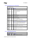
Table 131. Vital Product Data (VPD) Address Register
• Primary byte offset: E7:E6h
• Secondary byte offset: E7:E6h
Bit Name R/W Description
8:0 VPD Addr R/W
Vital Product Data Address. Contains the VPD byte address of the serial
ROM location to be accessed. Valid VPD byte addresses are 17F: 000h.
VPD starts at base address 080h in the serial ROM. The VPD byte
address contained in this register is added to the VPD base address to
obtain the final serial ROM address.
14:9 Reserved R Reserved. Read Only as 0.
15 VPD Flag R/W
VPD Flag. Starts a VPD serial ROM access and indicates completion of
the operation.
• When written with a 0: A 4-byte serial ROM read is
performed starting at the VPD location indicated by bits
[8:0]. Note that this operation is not necessarily Dword
aligned. When the read is complete, the 21555 sets this bit
to a 1.
• When written with a 1: A 4-byte serial ROM write is
performed starting at the VPD location indicated by bits
[8:0]. Note that this operation is not necessarily Dword
aligned.
• When the write is complete, the 21555 sets this bit to a 0.
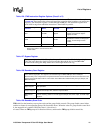
Table 132. VPD Data Register
• Primary byte offset: EB:E8h
• Secondary byte offset: EB:E8h
Bit Name R/W Description
31:0 VPD Data R/W
VPD Data. Contains the VPD read or write data. For a read, this register
should be read after a read operation was initiated and the 21555 has
returned the VPD Flag bit to a 1. For a write, this register should be
written with the write data before the operation is initiated with a write to
the VPD Address and VPD Flag bits. VPD read and write operations are
always 4
-byte operations.
Byte 0 contains the data corresponding to the starting VPD byte
address. Byte 1, 2, and 3 contain successive bytes. Note that Byte 0 is
not necessarily Dword aligned.


