S1D13705 Register Summary X27A-R-001-03
Page 1 01/02/13
Notes
1 These bits are used to identify the S1D13705 at power on / reset.
2 IO addresses are relative to the beginning of display memory.
3 Gray Shade/Color Mode Selection
4 Panel Data Format
5 High Performance Selection
6 Power Save Mode Selection
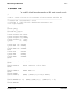
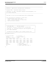
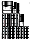
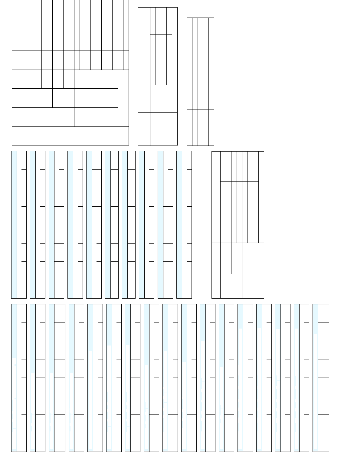
REG[00h] REVISION CODE REGISTER
1
IO address = 1FFE0h
2
, RO
Product Code = 001001 Revision Code = 00
Bit 5 Bit 4 Bit 3 Bit 2 Bit 1 Bit 0 Bit 1 Bit 0
REG[01h] MODE REGISTER 0 IO address = 1FFE1h, RW
TFT/STN Dual/Single Color/Mono
3
FPLine
Polarity
FPFrame
Polarity
Mask
FPSHIFT
Data Width
4
Bit 1 Bit 0
REG[02h] MODE REGISTER 1 IO address = 1FFE2h, RW
Bit-Per-Pixel
3
High
5
Performance
Input Clock
Div (CLKI/2)
Display
Blank
Frame
Repeat
Hw Video
Invert
Enable
Software
Video Invert
Bit 1 Bit 0
REG[03h] MODE REGISTER 2 IO address = 1FFE3h, RW
n/a n/a n/a n/a
LCDPWR
Override
Hardware
PS Enable
Sw Power Save
6
Bit 1 Bit 0
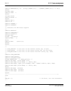
REG[04h] HORIZONTAL PANEL SIZE REGISTER IO address = 1FFE4h, RW
n/a
Horizontal Panel Size = 8(REG + 1)
Bit 6 Bit 5 Bit 4 Bit 3 Bit 2 Bit 1 Bit 0
REG[05h] VERTICAL PANEL SIZE REGISTER (LSB) IO address = 1FFE5h, RW
Vertical Panel Size = (REG[05h], REG[06h]) + 1
Bit 7 Bit 6 Bit 5 Bit 4 Bit 3 Bit 2 Bit 1 Bit 0
REG[06h] VERTICAL PANEL SIZE REGISTER (MSB) IO address = 1FFE6h, RW
n/a n/a n/a n/a n/a n/a
Vertical Panel Size
Bit 9 Bit 8
REG[07h] FPLINE START POSITION IO address = 1FFE7h, RW
n/a n/a n/a
FPLine Start Position = 8(REG[07h] + 2)
Bit 4 Bit 3 Bit 2 Bit 1 Bit 0
REG[08h] HORIZONTAL NON-DISPLAY PERIOD IO address = 1FFE8h, RW
n/a n/a n/a
Horizontal Non-Display Period = 8(REG + 4)
Bit 4 Bit 3 Bit 2 Bit 1 Bit 0
REG[09h] FPFRAME START POSITION IO address = 1FFE9h, RW
n/a n/a
FPFrame Start Position
Bit 5 Bit 4 Bit 3 Bit 2 Bit 1 Bit 0
REG[0Ah] VERTICAL NON-DISPLAY PERIOD REGISTER IO address = 1FFEAh, RW
Vert Non-
Disp Status
n/a
Vertical Non-Display Period
Bit 5 Bit 4 Bit 3 Bit 2 Bit 1 Bit 0
REG[0Bh] MOD RATE REGISTER IO address = 1FFEBh, RW
n/a n/a
MOD Rate
Bit 5 Bit 4 Bit 3 Bit 2 Bit 1 Bit 0
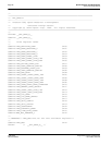
REG[0Ch] SCREEN 1 START WORD ADDRESS REGISTER (LSB) IO address = 1FFECh, RW
Screen 1 Start Word Address = (REG[0Ch], REG[0Dh], REG[10] bit 1)
Bit 7 Bit 6 Bit 5 Bit 4 Bit 3 Bit 2 Bit 1 Bit 0
REG[0Dh] SCREEN 1 START WORD ADDRESS REGISTER (MSB) IO address = 1FFEDh, RW
Screen 1 Start Word Address
Bit 15 Bit 14 Bit 13 Bit 12 Bit 11 Bit 10 Bit 9 Bit 8
REG[0Eh] SCREEN 2 START WORD ADDRESS REGISTER (LSB) IO address = 1FFEEh, RW
Screen 2 Start Word Address = (REG[0E], REG[0Fh], REG[10] bit 4)
Bit 7 Bit 6 Bit 5 Bit 4 Bit 3 Bit 2 Bit 1 Bit 0
REG[0Fh] SCREEN 2 START WORD ADDRESS REGISTER (MSB) IO address = 1FFEFh, RW
Screen 2 Start Word Address
Bit 15 Bit 14 Bit 13 Bit 12 Bit 11 Bit 10 Bit 9 Bit 8
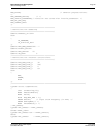
REG[10h] SCREEN START ADDRESS OVERFLOW REGISTER) IO address = 1FFF0h, RW
Screen 2
Start Add
Bit 16
Screen 1
Start Add
Bit 16
REG[11h] MEMORY ADDRESS OFFSET REGISTER IO address = 1FFF1h, RW
Memory Address Offset
Bit 7 Bit 6 Bit 5 Bit 4 Bit 3 Bit 2 Bit 1 Bit 0
REG[12h] SCREEN 1 VERTICAL SIZE REGISTER (LSB) IO address = 1FFF2h, RW
Screen 1 Vertical Size = (REG[12h], REG[13h])
Bit 7 Bit 6 Bit 5 Bit 4 Bit 3 Bit 2 Bit 1 Bit 0
REG[13h] SCREEN 1 VERTICAL SIZE REGISTER (MSB) IO address = 1FFF3h, RW
n/a n/a n/a n/a n/a n/a
Screen 1 Vertical Size
Bit 9 Bit 8
REG[15h] LOOK-UP TABLE ADDRESS REGISTER IO address = 1FFF5h, RW
Look-Up Table Address
Bit 7 Bit 6 Bit 5 Bit 4 Bit 3 Bit 2 Bit 1 Bit 0
REG[17h] LOOK-UP TABLE DATA REGISTER IO address = 1FFF7h, RW
Look-Up Table Data
n/a n/a n/a n/a
Bit 3 Bit 2 Bit 1 Bit 0
REG[18h] GPIO CONFIGURATION CONTROL REGISTER IO address = 1FFF8h, RW
n/a n/a n/a
GPIO4 Pin
IO Config
GPIO3 Pin
IO Config
GPIO2 Pin
IO Config
GPIO1 Pin
IO Config
GPIO0 Pin
IO Config
REG[19h] GPIO STATUS / CONTROL REGISTER IO address = 1FFF9h, RW
n/a n/a n/a
GPIO4 Pin
IO Status
GPIO3 Pin
IO Status
GPIO2 Pin
IO Status
GPIO1 Pin
IO Status
GPIO0 Pin
IO Status
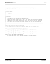
REG[1Ah] SCRATCH PAD REGISTER IO address = 1FFFAh, RW
Scratch Pad Register
Bit 7 Bit 6 Bit 5 Bit 4 Bit 3 Bit 2 Bit 1 Bit 0
REG[1Bh] SWIVELVIEW MODE REGISTER IO address = 1FFFBh, RW
SwivelView
Mode En.
SwivelView
Mode Sel.
n/a n/a n/a reserved
SwivelView PCLK Select
Bit 1 Bit 0
REG[1Ch] LINE BYTE COUNT REGISTER IO address = 1FFFCh, RW
Line Byte Count
Bit 7 Bit 6 Bit 5 Bit 4 Bit 3 Bit 2 Bit 1 Bit 0
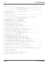
Color/Mono
REG[01] bit 5
Bit-Per-Pixel Bit 1
REG[02] bit 7
Bit-Per-Pixel Bit 0
REG[02] bit 6
Display Mode
1
0
0 2 Colors 1 Bit-Per-Pixel
1 4 Colors 2 Bit-Per-Pixel
1
0 16 Colors 4 Bit-Per-Pixel
1 256 Colors 8 Bit-Per-Pixel
0
0
0 2 Gray Shade 1 Bit-Per-Pixel
1 4 Gray Shade 2 Bit-Per-Pixel
1
0 16 Gray Shade 4 Bit-Per-Pixel
1 reserved
TFT/STN
REG[01]
bit 7
Color/
Mono
REG[01]
bit 5
Dual/
Single
REG[01]
bit 6
Data
Width
Bit 1
REG[01]
bit 1
Data
Width
Bit 0
REG[01]
bit 0
Function
0
0
0
0
0 Mono Single 4-bit LCD
1 Mono Single 8-bit LCD
1
0reserved
1reserved
1
0
0reserved
1 Mono Dual 8-bit LCD
1
0reserved
1reserved
1
0
0
0 Color Single 4-bit LCD
1 Color Single 8-bit LCD Format 1
1
0reserved
1 Color Single 8-bit LCD Format 2
1
0
0reserved
1 Color Dual 8-bit LCD
1
0reserved
1reserved
1 don’t care
0 9 bit TFT Panel
1 12 bit TFT Panel
High Performance
Bit-Per-Pixel
Bit 1
REG[02] bit 7
Bit-Per-Pixel
Bit 0
REG[02] bit 6
Display Modes
0
0
0 MClk = PClk/8 1 bit-per-pixel
1 MClk = PClk/4 2 bit-per-pixel
1
0 MClk = PClk/2 4 bit-per-pixel
1 MClk = PClk 8 bit-per-pixel
1XX MClk = PClk
Power Save Bit 1 Power Save Bit 0 Mode
0 0 Power Save Mode 1
0 1 reserved
1 0 reserved
1 1 Normal Operation
S1D13705 Register Summary X27A-R-001-03


