Epson Research and Development Page 11
Vancouver Design Center
13705CFG Configuration Program S1D13705
Issue Date: 02/03/11 X27A-B-001-03
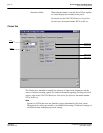
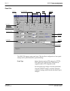
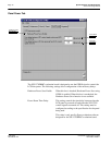
The S1D13705 uses one clock input known as CLKI. The pixel clock (PCLK) and the
memory clock (MCLK) are both derived from CLKI.
CLKI This setting determines the frequency of CLKI. CLKI is
the source for both PCLK and MCLK.
The CLKI frequency must be selected from the drop
down list or by entering the desired frequency in MHz.
The actual CLKI frequency used for configuration is
displayed in blue in the Actual section.
CLKI/2 Selecting this box divides the input clock, CLKI, in half
for internal S1D13705 operations.
PCLK These settings confirm the signal source and input clock
divisor for the pixel clock (PCLK).
Source The PCLK source is CLKI.
Divide The divide ratio for the clock source signal is 1:1.
Timing This field shows the actual PCLK used by the configu-
ration process.
MCLK These settings confirm the signal source and input clock
divisor for the memory clock (MCLK).
Source The MCLK source is CLKI.
Divide The divide ratio for the clock source signal is 1:1.
Timing This field shows the actual MCLK frequency used by
the configuration process.


