Epson Research and Development Page 83
Vancouver Design Center
Hardware Functional Specification S1D13705
Issue Date: 02/02/01 X27A-A-001-10
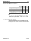
13.3 Power Save Mode Function Summary
Note
When FPDAT[11:8] are designated as GPIO outputs, the output state prior to enabling
the Power Save Mode is maintained. When FPDAT[11:8] are designated as GPIO in-
puts, unused inputs must be tied to either IO V
DD
or GND - see Table 5.5 “LCD Inter-
face Pin Mapping,” on page 23.
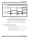
13.4 Panel Power Up/Down Sequence
After chip reset or when entering/exiting a power save mode, the Panel Interface signals
follow a power on/off sequence shown below. This sequence is essential to prevent damage
to the LCD panel.
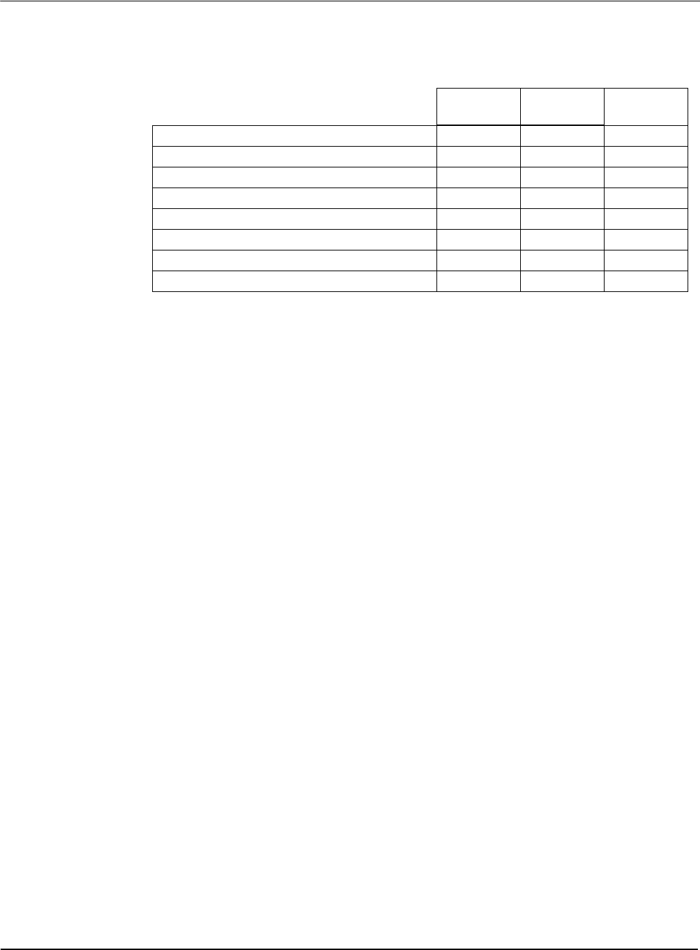
Table 13-4: Power Save Mode Function Summary
Hardware
Power Save
Software
Power Save
Normal
IO Access Possible? No Yes Yes
Memory Access Possible? No Yes Yes
Look-Up Table Registers Access Possible? No No Yes
Sequence Controller Running? No No Yes
Display Active? No No Yes
LCDPWR Inactive Inactive Active
FPDAT[11:0], FPSHIFT (see note) Forced Low Forced Low Active
FPLINE, FPFRAME, DRDY Forced Low Forced Low Active


