


Page 26 Epson Research and Development
Vancouver Design Center
S1D13705 Interfacing to the Motorola ‘Dragonball’ Family of Microprocessors
X27A-G-007-04 Issue Date: 01/02/13
4.4 MC68VZ328 To S1D13705 Interface
4.4.1 Hardware Description
The interface between the MC68VZ328 and the S1D13705 can be implemented using
either the MC68K #1 or Generic #1 host bus interface of the S1D13705.
Using The MC68K #1 Host Bus Interface
The MC68VZ328 multiplexes dual functions on some of its bus control pins (specifically
UDS
, LDS, and DTACK). In implementations where all of these pins are available for use
as bus control pins, then the S1D13705 interface is a straightforward implementation of the
“MC68K #1” host bus interface. Since AS
is not provided by the DragonballVZ, CSB1 is
connected to BS# and indicates that a valid address is on the bus.
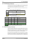
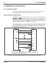
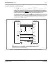
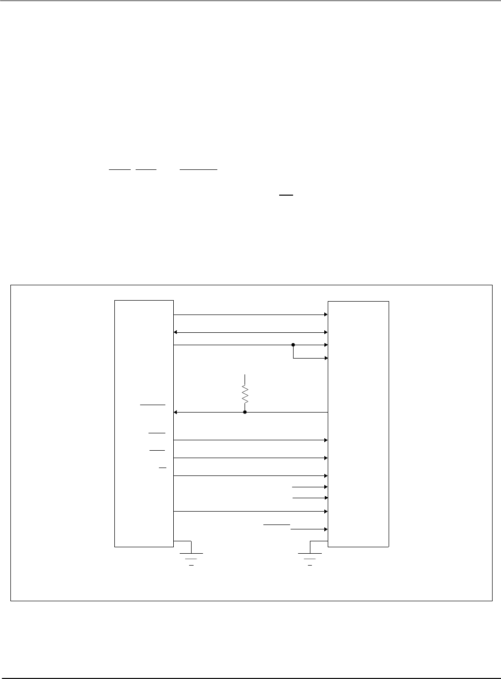
The following diagram shows a typical implementation of the MC68VZ328 to S1D13705
using the MC68K #1 host bus interface. For further information on the MC68K #1 host bus
interface and AC Timing, refer to the S1D13705 Hardware Functional Specification,
document number X27A-A-001-xx.
Figure 4-1: Typical Implementation of MC68VZ328 to S1D13705 Interface - MC68K #1
MC68VZ328 S1D13705
A[16:0]
D[15:0]
DTACK
UDS
LDS
R/W
CLK0
AB[16:1]
DB[15:0]
CS#
WAIT#
WE1#
AB0
RD/WR#
RD#
BUSCLK
RESET#
Vcc
1K
CSB1
BS#
Vcc
System RESET
WE0##
Vcc
Note:
When connecting the S1D13705 RESET# pin, the system designer should be aware of all
conditions that may reset the S1D13705 (e.g. CPU reset can be asserted during wake-up
from power-down modes, or during debug states).