Page 20 Epson Research and Development
Vancouver Design Center
S1D13705 Interfacing to the Motorola ‘Dragonball’ Family of Microprocessors
X27A-G-007-04 Issue Date: 01/02/13
3.4.2 S1D13705 Hardware Configuration
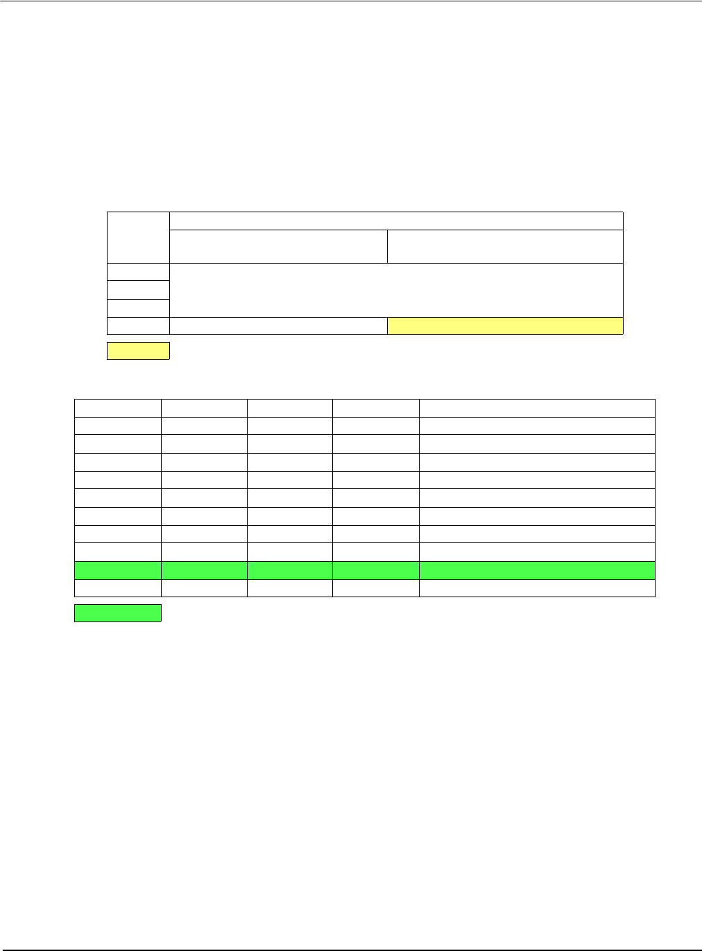
The S1D13705 uses CNF3 through CNF0 and BS# to allow selection of the bus mode and
other configuration data on the rising edge of RESET#. Refer to the S1D13705 Hardware
Functional Specification, document number X27A-A-001-xx for details.
The tables below show those configuration settings important to the Generic #1 host bus
interface.
3.4.3 MC68EZ328 Chip Select Configuration
The S1D13705 requires a 128K byte address space for the display buffer and its internal
registers. To accommodate this block size, it is preferable (but not required) to use one of
the chip selects from groups A or B. Groups A and B can have a size range of 128K bytes
to 16M bytes and groups C and D have a size range of 32K bytes to 16M bytes. Therefore,
any chip select other than CSA0 would be suitable for the S1D13705 interface.
In the example interface, chip select CSB0 is used to control the S1D13705. A 128K byte
address space is used with the S1D13705 control registers mapped into the top 32 bytes of
the 128K byte block and the 80K bytes of display buffer mapped to the starting address of
the block. The chip select should have its RO (Read Only) bit set to 0, its BSW (Bus Data
Table 3-2: Summary of Power-On/Reset Options
S1D1370
5
Pin Name
value on this pin at the rising edge of RESET# is used to configure: (1/0)
01
CNF0
See Table 2-3: “Host Bus Interface Selection” CNF1
CNF2
CNF3 Little Endian
Big Endian
= configuration for MC68EZ328 support
Table 3-3: Host Bus Interface Selection
CNF2 CNF1 CNF0 BS# Host Bus Interface
0 0 0 X SH-4 interface
0 0 1 X SH-3 interface
010Xreserved
0 1 1 X MC68K #1, 16-bit
100Xreserved
1 0 1 X MC68K #2, 16-bit
1100reserved
1101reserved
1 1 1 0 Generic #1, 16-bit
1 1 1 1 Generic #2, 16-bit
= configuration for MC68EZ328 using Generic #1 host bus interface


