Epson Research and Development Page 55
Vancouver Design Center
Hardware Functional Specification S1D13705
Issue Date: 02/02/01 X27A-A-001-10
8 Registers
8.1 Register Mapping
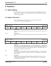
The S1D13705 registers are located in the upper 32 bytes of the 128K byte S1D13705
address range. The registers are accessible when CS# = 0 and AB[16:0] are in the range
1FFE0h through 1FFFFh.
8.2 Register Descriptions
Unless specified otherwise, all register bits are reset to 0 during power up.
All bits marked n/a should be programmed 0.
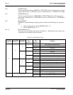
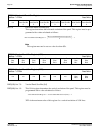
bits 7-2 Product Code
This is a read-only register that indicates the product code of the chip. The product code is
001001.
bits 1-0 Revision Code
This is a read-only register that indicates the revision code of the chip. The revision code is
00.
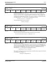
bit 7 TFT/STN
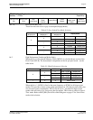
When this bit = 0, STN (passive) panel mode is selected. When this bit = 1, TFT/D-TFD
panel mode is selected. If TFT/D-TFD panel mode is selected, Dual/Single (REG[01h] bit
6) and Color/Mono (REG[01h] bit5) are ignored. See Table 8-1: “Panel Data Format” for a
comprehensive description of panel selection.
bit 6 Dual/Single
When this bit = 0, Single LCD panel drive is selected. When this bit = 1, Dual LCD panel
drive is selected. See Table 8-1: “Panel Data Format” for a comprehensive description of
panel selection.
bit 5 Color/Mono
When this bit = 0, Monochrome LCD panel drive is selected. When this bit = 1, Color
LCD panel drive is selected. See Table 8-1: “Panel Data Format” for a comprehensive
description of panel selection.
REG[00h] Revision Code Register
Address = 1FFE0h Read Only.
Product Code
Bit 5
Product Code
Bit 4
Product Code
Bit 3
Product Code
Bit 2
Product Code
Bit 1
Product Code
Bit 0
Revision
Code Bit 1
Revision
Code Bit 0
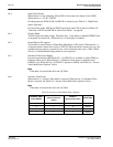
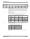
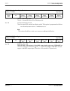
REG[01h] Mode Register 0
Address = 1FFE1h Read/Write.
TFT/STN Dual/Single Color/Mono
FPLine
Polarity
FPFrame
Polarity
Mask
FPSHIFT
Data Width
Bit 1
Data Width
Bit 0


