Epson Research and Development Page 13
Vancouver Design Center
Interfacing to the Toshiba MIPS TMPR3912 Microprocessor S1D13705
Issue Date: 01/02/13 X27A-G-004-02
The “Generic #2” host interface control signals of the S1D13705 are asynchronous with
respect to the S1D13705 bus clock. This gives the system designer full flexibility to choose
the appropriate source (or sources) for CLKI and BCLK. The choice of whether both clocks
should be the same, and whether to use DCLKOUT (divided) as clock source, should be
based on the desired:
• pixel and frame rates.
• power budget.
•part count.
• maximum S1D13705 clock frequencies.
The S1D13705 also has internal clock dividers providing additional flexibility.
4.2 Memory Mapping and Aliasing
In this example implementation the TMPR3912 control signal CARDREG* is ignored;
therefore the S1D13705 takes up the entire PC Card slot 1.
The S1D13705 requires an addressing space of 128K bytes. The on-chip display memory
occupies the range 0 through 13FFFh. The registers occupy the range 1FFE0h through
1FFFFh. The TMPR3912 demultiplexed address lines A17 and above are ignored, thus the
S1D13705 is aliased 512 times at 128K byte intervals over the 64M byte PC Card slot #1
memory space.
Note
If aliasing is undesirable, additional decoding circuitry must be added.
4.3 S1D13705 Configuration
The S1D13705 is configured at power up by latching the state of the CNF[3:0] pins. Pin
BS# also plays a role in host bus interface configuration. For details on configuration, refer
to the S1D13705 Hardware Functional Specification, document number X27A-A-001-xx.
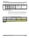
The table below shows those configuration settings relevant to the direct connection
approach.
Table 4-1: S1D13705 Configuration for Direct Connection
S1D13705
Configuration
Pin
Value hard wired on this pin is used to configure:
1 (IO V
DD
)0 (V
SS
)
BS#
Generic #2 Generic #1
CNF3 Big Endian
Little Endian
CNF[2:0]
111: Generic #1 or #2
= configuration for Toshiba TMPR3912 host bus interface


