Epson Research and Development Page 19
Vancouver Design Center
S5U13705B00C Rev. 2.0 Evaluation Board User Manual S1D13705
Issue Date: 2002/09/16 X27A-G-014-02
6 Technical Description
6.1 PCI Bus Support
The S1D13705 does not have on-chip PCI bus interface support. The S1D13705B00C uses
the PCI Bridge FPGA to support the PCI bus. When using the PCI Bridge FPGA, a
Windows device driver is required, see Section 7, “Software” on page 22 for further infor-
mation on available software and drivers.
6.2 Direct Host Bus Interface Support
The S5U13705B00C is specifically designed to work using the PCI Bridge FPGA in a
standard PCI bus environment. However, the S1D13705 directly supports many other host
bus interfaces. Connectors H1 and H2 provide the necessary IO pins to interface to these
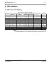
host buses. For further information on the host bus interfaces supported, see “CPU
Interface” on page 15.
Note
The PCI Bridge FPGA must be disabled using JP5 in order for direct host bus interface
to operate properly.
6.3 S1D13705 Embedded Memory
The S1D13705 has 80K bytes of embedded SRAM. The 80K byte display buffer address
space is directly and contiguously available through the 17-bit address bus.
The S1D13705 registers are located in the upper 32 bytes of the 128K byte address range
of S1D13705.
6.4 Adjustable LCD Panel Positive Power Supply (VDDH)
For those LCD panels requiring a positive power supply to provide between +23V and
+40V (Iout = 45mA) a power supply has been provided as an integral part of this design.
The VDDH power supply can be adjusted by R15 to provide an output voltage from +23V
to +40V and is enabled and disabled by the active high LCDPWR control signal of
S1D13705 and inverted externally.
Determine the panel’s specific power requirements and set the potentiometer accordingly
before connecting the panel.


