


Epson Research and Development Page 19
Vancouver Design Center
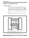
Interfacing to the Motorola MPC821 Microprocessor S1D13705
Issue Date: 01/02/13 X27A-G-010-02
4.4 MPC821 Chip Select Configuration
The DRAM on the MPC821 ADS board extends from address 0 through 3F FFFFh, so the
S1D13705 is addressed starting at 40 0000h. The S1D13705 uses a 128K byte segment of
memory starting at this address, with the first 80K bytes used for the display buffer and the
upper 32 bytes of this memory block used for the S1D13705 internal registers.
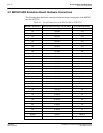
Chip select 4 is used to control the S1D13705. The following options are selected in the
base address register (BR4):
• BA (0:16) = 0000 0000 0100 0000 0 – set starting address of S1D13705 to 40 0000h
• AT (0:2) = 0 – ignore address type bits
• PS (0:1) = 1:0 – memory port size is 16 bits
• PARE = 0 – disable parity checking
• WP = 0 – disable write protect
• MS (0:1) = 0:0 – select General Purpose Chip Select module to control this chip select
• V = 1 – set valid bit to enable chip select
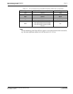
The following options were selected in the option register (OR4):
• AM (0:16) = 1111 1111 1100 0000 0 – mask all but upper 10 address bits; S1D13705
consumes 4M byte of address space
• ATM (0:2) = 0 – ignore address type bits
• CSNT = 0 – normal CS
/WE negation
• ACS (0:1) = 1:1 – delay CS
assertion by ½ clock cycle from address lines
• BI = 1 – assert Burst Inhibit
• SCY (0:3) = 0 – wait state selection; this field is ignored since external transfer
acknowledge is used; see SETA below
• SETA = 1 – the S1D13705 generates an external transfer acknowledge using the
WAIT# line
• TRLX = 0 – normal timing
• EHTR = 0 – normal timing