Epson Research and Development Page 13
Vancouver Design Center
Interfacing to the NEC VR4181A™ Microprocessor S1D13705
Issue Date: 01/02/13 X27A-G-013-02
The host interface control signals of the S1D13705 are asynchronous with respect to the
S1D13705 bus clock. This gives the system designer full flexibility to choose the appro-
priate source (or sources) for CLKI and BCLK. The choice of whether both clocks should
be the same, and whether an external or internal clock divider is needed, should be based
on the desired:
• pixel and frame rates.
• power budget.
•part count.
• maximum S1D13705 clock frequencies.
The S1D13705 also has internal clock dividers providing additional flexibility.
4.2 S1D13705 Hardware Configuration
The S1D13705 uses CNF3 through CNF0 and BS# to allow selection of the bus mode and
other configuration data on the rising edge of RESET#. Refer to the S1D13705 Hardware
Functional Specification, document number X27A-A-001-xx for details.
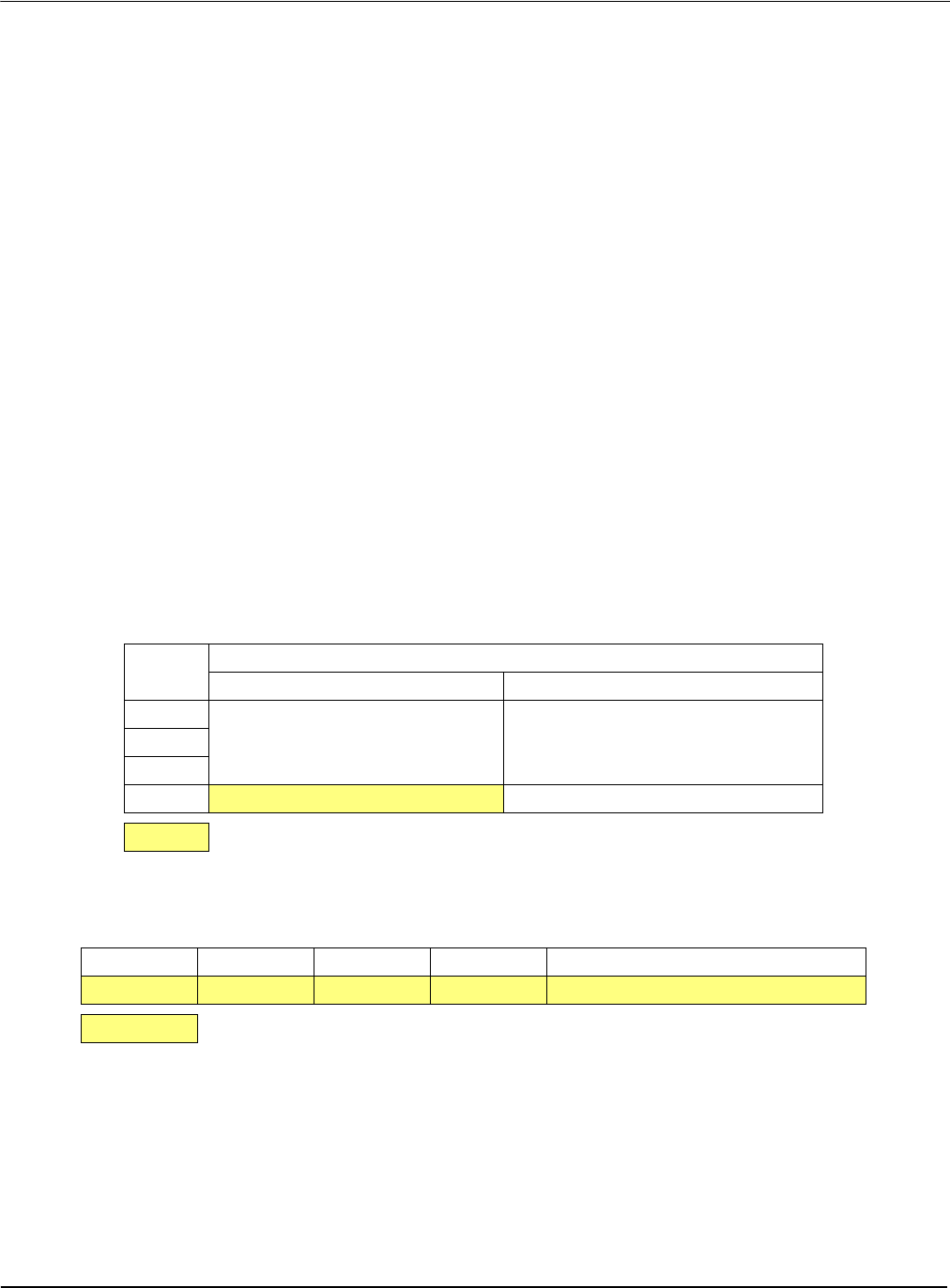
The tables below show those configuration settings important to the Generic #2 host bus
interface.
Table 4-1: Summary of Power-On/Reset Options
Signal
value on this pin at the rising edge of RESET# is used to configure: (0/1)
01
CNF0
See “Host Bus Selection” table below See “Host Bus Selection” table belowCNF1
CNF2
CNF3
Little Endian Big Endian
= configuration for NEC VR4181A support
Table 4-2: Host Bus Selection
CNF2 CNF1 CNF0 BS# Host Bus Interface
1 1 1 1 Generic #2, 16-bit
= configuration for NEC VR4181A support


