Page 8 Epson Research and Development
Vancouver Design Center
S1D13705 13705CFG Configuration Program
X27A-B-001-03 Issue Date: 02/03/11
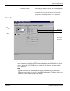
Decode Addresses Selecting one of the listed evaluation platforms changes
the values for the “Register address” and “Display
buffer address” fields. The values used for each evalu-
ation platform are examples of possible implementa-
tions as used by the Epson S1D13705 evaluation board.
If your hardware implementation differs from the
addresses used, select the User-Defined option and
enter the correct addresses for “Register address” and
“Display buffer address”.
Register Address The physical address of the start of register decode
space (in hexadecimal).
This field is automatically set according to the Decode
Address unless the “User-Defined” decode address is
selected.
Display Buffer Address The physical address of the start of display buffer
decode space (in hexadecimal).
This field is automatically set according to the Decode
Address unless the “User-Defined” decode address is
selected.
Note
When “Epson S5U13705B00C Rev. 2 Evaluation Board” is selected, the register and
display buffer addresses are blanked because the evaluation board uses the PCI interface
and the decode addresses are determined by the system BIOS during boot-up.
If using the S1D13705 Evaluation Board on a PCI based platform, both Windows and
the S1D13XXX device driver must be installed. For further information on the
S1D13XXX device driver, see the S1D13XXX Windows 32-bit Windows Device Driver
Installation Guide, document number X00A-E-003-xx.


