Epson Research and Development Page 13
Vancouver Design Center
Interfacing to the PC Card Bus S1D13705
Issue Date: 01/02/13 X27A-G-009-02
4.2 S1D13705 Hardware Configuration
The S1D13705 uses CNF3 through CNF0 and BS# to allow selection of the bus mode and
other configuration data on the rising edge of RESET#. Refer to the S1D13705 Hardware
Functional Specification, document number X27A-A-001-xx for details.
The tables below show only those configuration settings important to the PC Card host bus
interface.
4.3 Register/Memory Mapping
The S1D13705 is a memory mapped device. The S1D13705 memory may be addressed
starting at 0000h, or on consecutive 128K byte blocks, and its internal registers are located
in the upper 32 bytes of the 128K byte block (i.e. REG[0] = 1FFE0h).
While the PC Card socket provides 64M bytes of memory address space, the S1D13705
only needs a 128K byte block of memory to accommodate its 80K byte display buffer and
its 32 byte register set. For this reason only address bits A[16:0] are used while A[25:17]
are ignored. Because the entire 64M bytes of memory is available, the S1D13705’s memory
and registers will be aliased every 128K bytes for a total of 512 times.
Note
If aliasing is not desirable, the upper addresses must be fully decoded.
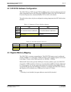
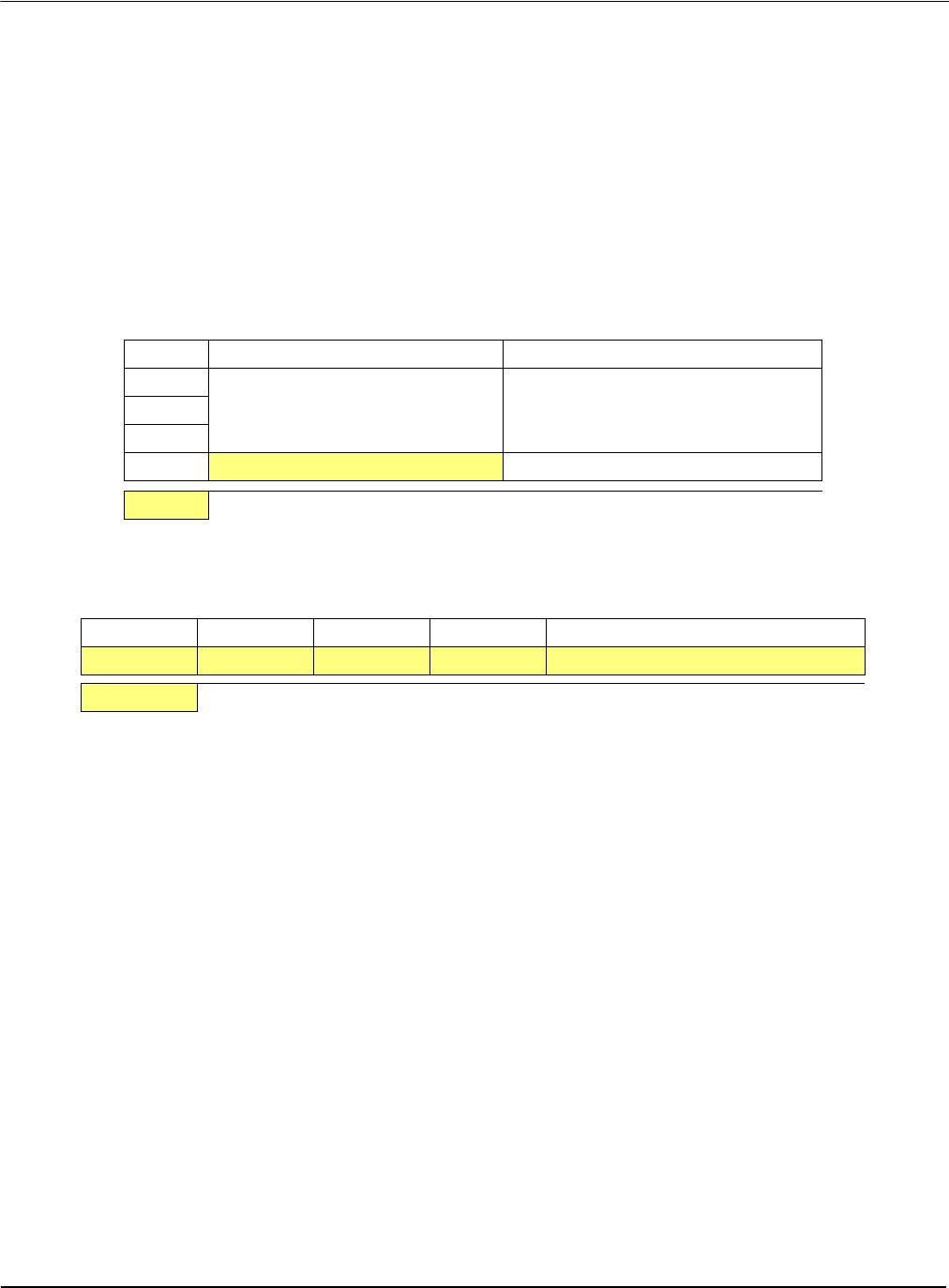
Table 4-1: Summary of Power-On/Reset Options
Signal Low High
CNF0
See “Host Bus Selection” table below See “Host Bus Selection” table belowCNF1
CNF2
CNF3
Little Endian Big Endian
= configuration for PC Card host bus interface
Table 4-2: Host Bus Interface Selection
CNF2 CNF1 CNF0 BS# Host Bus Interface
1 1 1 1 Generic #2, 16-bit
= configuration for PC Card host bus interface


