


Page 84 Epson Research and Development
Vancouver Design Center
S1D13705 Hardware Functional Specification
X27A-A-001-10 Issue Date: 02/02/01
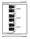
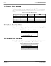
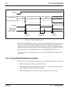
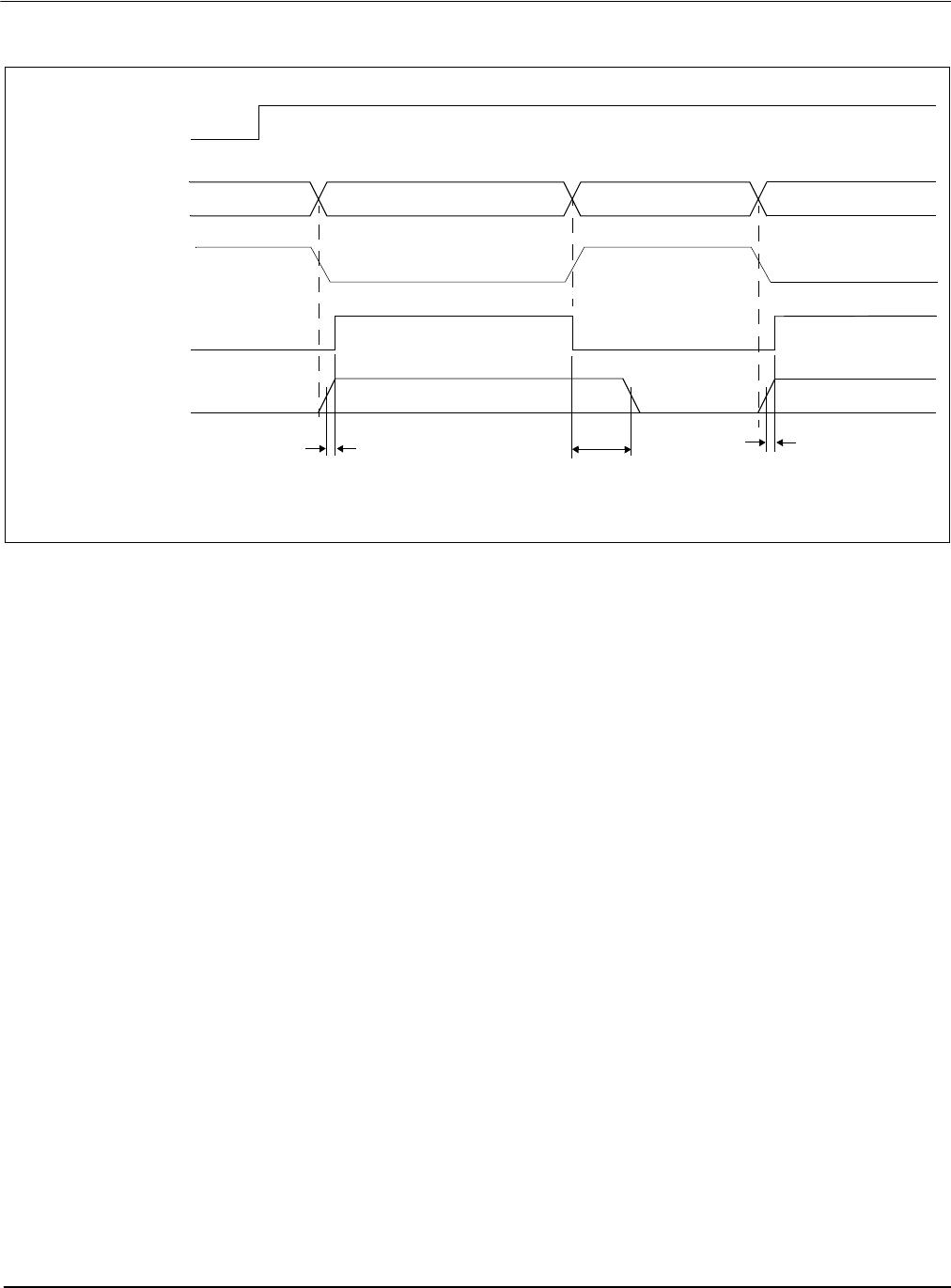
Figure 13-1: Panel On/Off Sequence
After chip reset, LCDPWR is inactive and the rest of the panel interface output signals are
held “low”. Software initializes the chip (i.e. programs all registers except the Look-Up
Table registers) and then programs REG[03h] bits [1:0] to 11b. This starts the power-up
sequence as shown. The power-up/power-down sequence delay is 127 frames. The Look-
Up Table registers may be programmed any time after REG[03h] bits[1:0] = 11b.
The power-up/power-down sequence also occurs when exiting/entering Software Power
Save Mode.
13.5 Turning Off BCLK Between Accesses
BCLK may be turned off (held low) between accesses if the following rules are observed:
1. BCLK must be turned off/on in a glitch free manner
2. BCLK must continue for a period equal to [8T
BCLK
+ 12T
MCLK
] after the end of the
access (RDY# asserted or WAIT# deasserted).
3. BCLK must be present for at least one T
BCLK
before the start of an access.
RESET#
LCDPWR
Panel Interface
Output Signals
(except LCDPWR)
0 frame 127 frames 0 frame
Power Save Mode
power-down power-uppower-up
Software Power Save
00 11 00 11
Hardware Power Save
REG[03h] bits [1:0]
or