


Page 16 Epson Research and Development
Vancouver Design Center
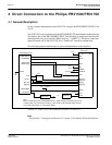
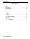
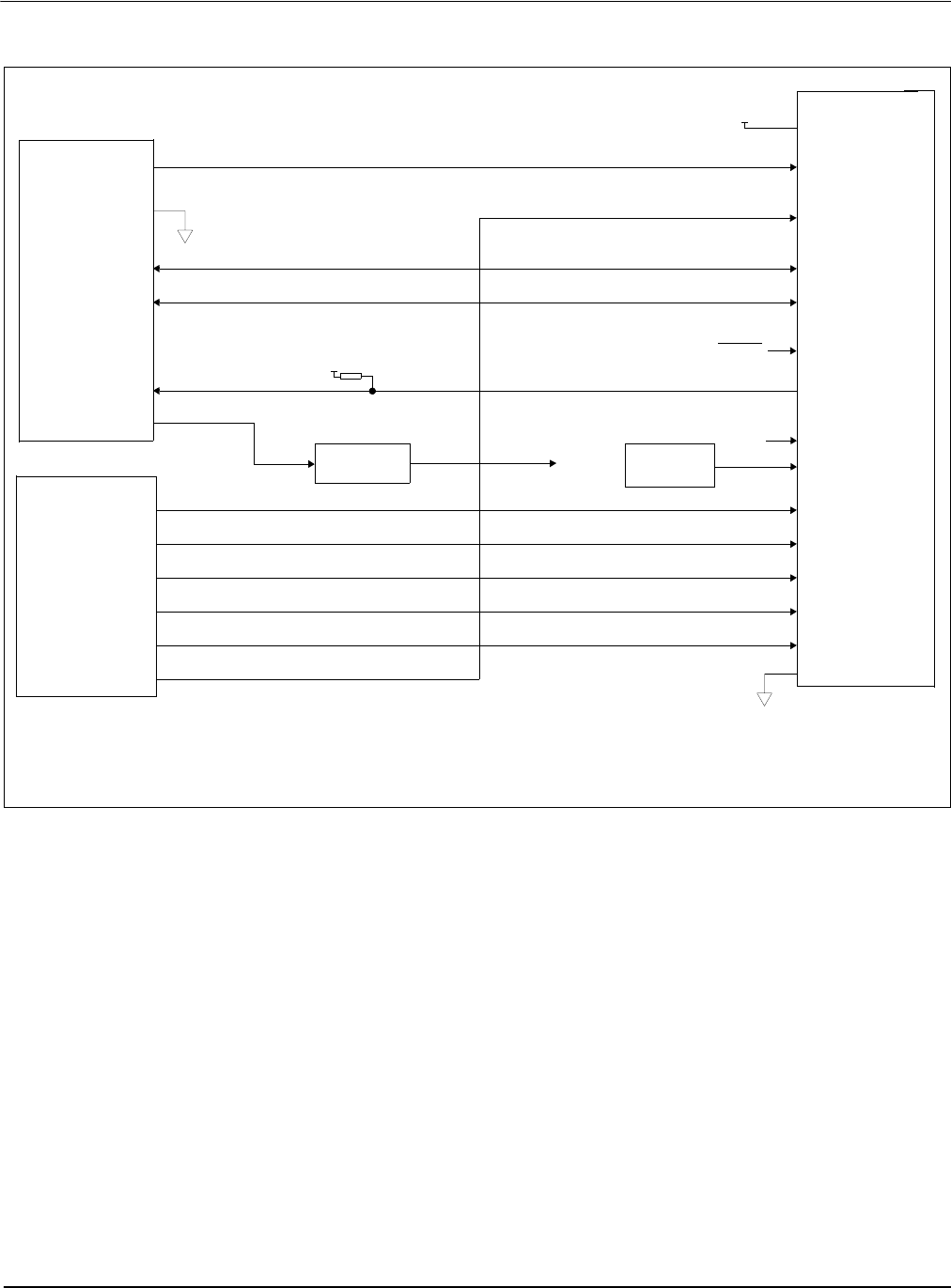
S1D13705 Interfacing to the Philips MIPS PR31500/PR31700 Processor
X27A-G-012-02 Issue Date: 01/02/13
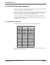
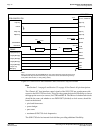
Figure 5-1: S1D13705 to PR31500/PR31700 Connection Using an IT8368E
Note
See Section 3.1 on page 9 and Section 3.2 on page 10 for Generic #1 pin descriptions.
The “Generic #1” host interface control signals of the S1D13705 are asynchronous with
respect to the S1D13705 bus clock. This gives the system designer full flexibility to choose
the appropriate source (or sources) for CLKI and BCLK. The choice of whether both clocks
should be the same, and whether to use DCLKOUT (divided) as clock source, should be
based on the desired:
• pixel and frame rates.
• power budget.
• part count.
• maximum S1D13705 clock frequencies.
The S1D13705 also has internal clock dividers providing additional flexibility.
IT8368E
S1D13705
HA[12:0]
AB[12:0]
HD[31:24]
DB[7:0]
LHA[23]/MFIO[10]
WE1#
WE0#
RD/WR#
RD#
CS#
LHA[22]/MFIO[9]
LHA[21]/MFIO[8]
LHA[20]/MFIO[7]
LHA[19]/MFIO[6]
WAIT#
/CARDxWAIT
RESET#
AB[16:13]
PR31500/PR31700
HD[23:16]
DB[15:8]
DCLKOUT
ENDIAN
System RESET
LHA[16:13]/
Oscillator
...or...
pull-up
V
DD
BCLK
CLKI
See text
Clock divider
BS#
IO V
DD
, CORE V
DD
+3.3V
MFIO[3:0]
Note:
When connecting the S1D13705 RESET# pin, the system designer should be aware of all
conditions that may reset the S1D13705 (e.g. CPU reset can be asserted during wake-up
from power-down modes, or during debug states).