Epson Research and Development Page 27
Vancouver Design Center
Interfacing to the Motorola ‘Dragonball’ Family of Microprocessors S1D13705
Issue Date: 01/02/13 X27A-G-007-04
Using The Generic #1 Host Bus Interface
The DTACK
signal must be made available for the S1D13705, since it inserts a variable
number of wait states depending upon CPU/LCD synchronization and the LCD panel
display mode. WAIT# must be inverted (using an inverter enabled by CS#) to make it an
active high signal and thus compatible with the MC68VZ328 architecture. A single resistor
is used to pull up the WAIT# (DTACK
) signal when terminating the bus cycle.
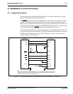
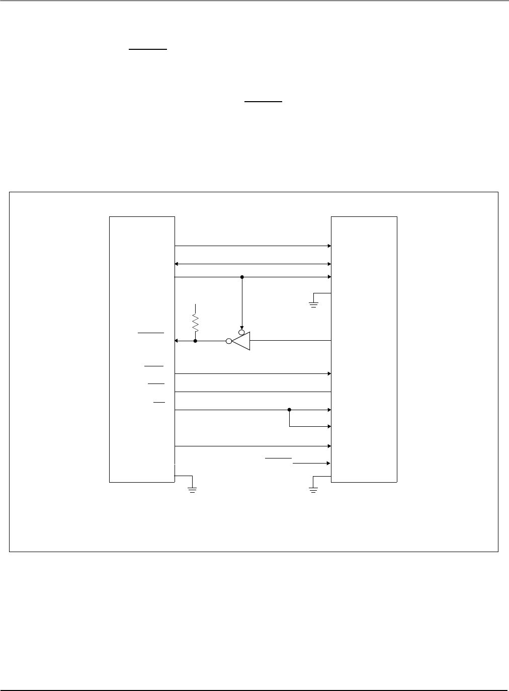
The following diagram shows a typical implementation of the MC68VZ328 to S1D13705
using the Generic #1 host bus interface. For further information on the Generic #1 host bus
interface and AC Timing, refer to the S1D13705 Hardware Functional Specification,
document number X27A-A-001-xx.
Figure 4-2: Typical Implementation of MC68VZ328 to S1D13705 Interface - Generic #1
MC68VZ328
S1D13705
A[16:0]
D[15:0]
DTACK
UWE
LWE
OE
CLK0
AB[16:0]
DB[15:0]
CS#
WAIT#
WE1#
WE0#
RD/WR#
RD#
BUSCLK
RESET#
Vcc
1K
CSB1
BS#
Note:
When connecting the S1D13705 RESET# pin, the system designer should be aware of all
conditions that may reset the S1D13705 (e.g. CPU reset can be asserted during wake-up
from power-down modes, or during debug states).
System RESET


