Epson Research and Development Page 15
Vancouver Design Center
Interfacing to the Motorola MPC821 Microprocessor S1D13705
Issue Date: 01/02/13 X27A-G-010-02
4 MPC821 to S1D13705 Interface
4.1 Hardware Description
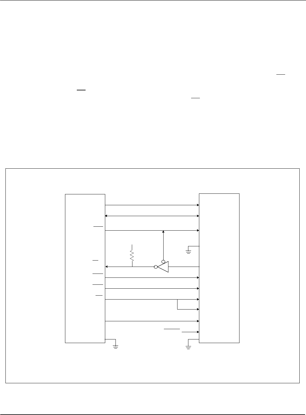
The interface between the S1D13705 and the MPC821 requires minimal glue logic. One
inverter is required to change the polarity of the WAIT# signal (an active low signal) to
insert wait states in the bus cycle. The MPC821 Transfer Acknowledge signal (TA
) is an
active low signal which ends the current bus cycle. The inverter is enabled using CS# so
that TA
is not driven by the S1D13705 during non-S1D13705 bus cycles. A single resistor
is used to speed up the rise time of the WAIT# (TA
) signal when terminating the bus cycle.
BS# (bus start) is not used in this implementation and should be tied low (connected to
GND).
The following diagram shows a typical implementation of the MPC821 to S1D13705
interface.
Figure 4-1: Typical Implementation of MPC821 to S1D13705 Interface
MPC821
S1D13705
A[15:31]
D[0:15]
CS4
TA
WE0
WE1
OE
SYSCLK
AB[16:0]
DB[15:0]
CS#
WAIT#
WE1#
WE0#
RD/WR#
RD#
BUSCLK
RESET#
Vcc
470
BS#
System RESET
Note:
When connecting the S1D13705 RESET# pin, the system designer should be aware of all
conditions that may reset the S1D13705 (e.g. CPU reset can be asserted during wake-up
from power-down modes, or during debug states).


