Page 14 Epson Research and Development
Vancouver Design Center
S1D13705 Interfacing to the NEC VR4102/VR4111 Microprocessor
X27A-G-008-02 Issue Date: 01/02/13
4.3 NEC VR4102/VR4111 Configuration
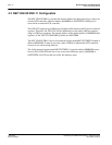
The NEC VR4102/VR4111 provides the internal address decoding necessary to map to an
external LCD controller. Physical address 0A000000h to 0AFFFFFFh (16M bytes) is
reserved for an external LCD controller.
The S1D13705 supports up to 80K bytes of display buffer memory and 32 bytes for internal
registers. Therefore, the S1D13705 will be shadowed over the entire 16M byte memory
range at 128K byte segments. The starting address of the display buffer is 0A000000h and
register 0 of the S1D13705 (REG[00h]) resides at 0A01FFE0h.
The NEC VR4102/VR4111 has a 16-bit internal register named BCUCNTREG2 located at
address 0B000002h. It must be set to the value of 0001h to indicate that LCD controller
accesses use a non-inverting data bus.
The 16-bit internal register named BCUCNTREG1, located at address 0B000000h, must
have bit D[13] (ISA/LCD bit) set to 0 to reserve the 16M bytes space, 0A000000h to
0AFFFFFFh, for LCD use and not as ISA bus memory space.


