Page 12 Epson Research and Development
Vancouver Design Center
S1D13705 Interfacing to an 8-bit Processor
X27A-G-015-01 Issue Date: 01/12/20
4.2 S1D13705 Hardware Configuration
The S1D13705 uses CNF4 through CNF0 and BS# to allow selection of the bus mode and
other configuration data on the rising edge of RESET#. Refer to the S1D13705 Hardware
Functional Specification, document number X27A-A-001-xx for details.
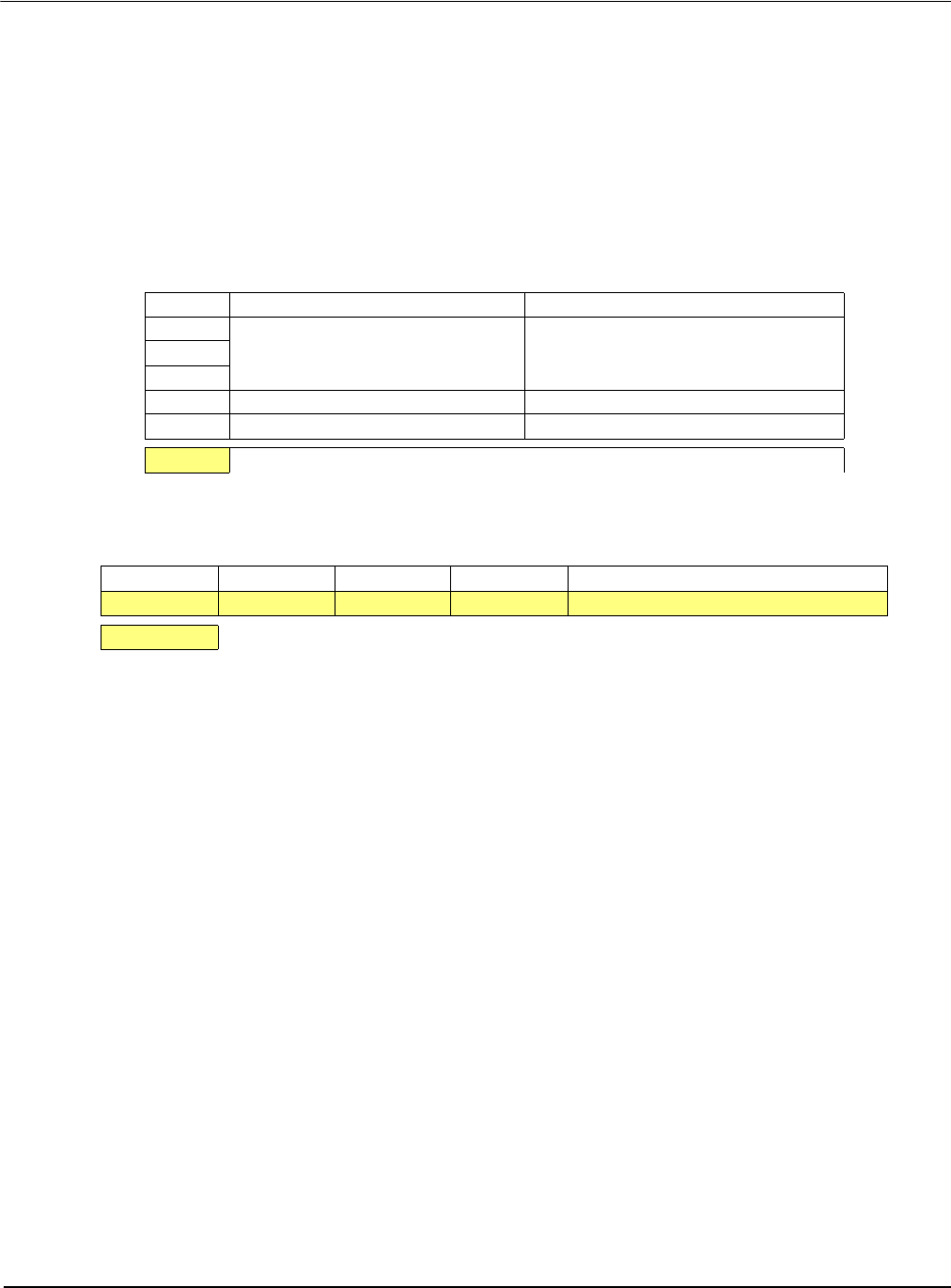
The tables below show only those configuration settings important to the 8-bit processor
interface. The endian must be selected based on the 8-bit processor used.
4.3 Register/Memory Mapping
The S1D13705 needs a 128K byte block of memory to accommodate its 80K byte display
buffer and its 32 byte register set. The starting memory address is located at 00000h of the
128K byte memory block while the internal registers are located in the upper 32 bytes of
this memory block. (i.e. REG[0]= 1FFE0h).
An external decoder can be used to decode the address lines and generate a chip select for
the S1D13705 whenever the selected 128K byte memory block is accessed. If the processor
supports a general chip select module, its internal registers can be programmed to generate
a chip select for the S1D13705 whenever the S1D13705 memory block is accessed.
Table 4-1: Configuration Settings
Signal Low High
CNF0
See “Host Bus Selection” table below See “Host Bus Selection” table belowCNF1
CNF2
CNF3
Little Endian Big Endian
CNF4 Active low LCDPWR signal Active high LCDPWR signal
= configuration for 8-bit processor host bus interface
Table 4-2: Host Bus Selection
CNF2 CNF1 CNF0 BS# Host Bus Interface
1 1 1 1 Generic #2, 16-bit
= required configuration for this application.


