Epson Research and Development Page 17
Vancouver Design Center
Interfacing to the Motorola ‘Dragonball’ Family of Microprocessors S1D13705
Issue Date: 01/02/13 X27A-G-007-04
select ceases to decode globally once this chip-select’s registers are programmed. Groups
C and D are special in that they can also control DRAM interfaces. These last two groups
have block size of 32K bytes to 4M bytes.
3.3 S1D13705 Host Bus Interface
This section is a summary of the host bus interface modes available on the S1D13705 that
may be used to interface to the MC68EZ328.
The S1D13705 implements a 16-bit interface to the host microprocessor which may operate
in one of several modes compatible with most of the popular embedded microprocessor
families. The interface mode that may be used for the MC68EZ328 is:
• Generic #1 (Chip Select, plus individual Read Enable/Write Enable for each byte).
3.3.1 Host Bus Pin Connection
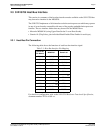
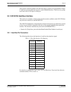
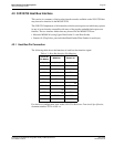
The following table shows the functions of each host bus interface signal.
For details on configuration, refer to the S1D13705 Hardware Functional Specification,
document number X27A-A-001-xx.
Table 3-1: Host Bus Interface Pin Mapping
S1D13705
Pin Names
Generic #1
AB[15:1] A[15:1]
AB0 A0
DB[15:0] D[15:0]
WE1# WE1#
CS# External Decode
BCLK BCLK
BS# connect to V
SS
RD/WR# RD1#
RD# RD0#
WE0# WE0#
WAIT# WAIT#
RESET# RESET#


