Epson Research and Development Page 67
Vancouver Design Center
Hardware Functional Specification S1D13705
Issue Date: 02/02/01 X27A-A-001-10
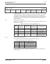
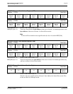
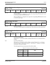
bits 4-0 GPIO[4:0] Status
When the GPIOn pin is configured as an input, the corresponding GPIO Status bit is used
to read the pin input. See REG[18h] above.
When the GPIOn pin is configured as an output, the corresponding GPIO Status bit is used
to control the pin output.
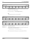
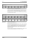
bits 7-0 Scratch Pad Register
This register contains general use read/write bits. These bits have no effect on hardware.
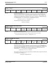
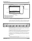
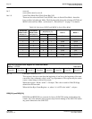
bit 7 SwivelView Mode Enable
When this bit = 1, SwivelView Mode is enabled. When this bit = 0, Landscape Mode is
enabled.
bit 6 SwivelView Mode Select
When this bit = 0, Default SwivelView Mode is selected. When this bit = 1, Alternate
SwivelView Mode is selected. See Section 12, “SwivelView™” on page 77 for further
information on SwivelView Mode.
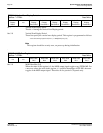
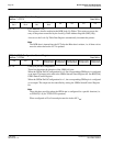
The following table shows the selection of SwivelView Mode.
REG[19h] GPIO Status/Control Register
Address = 1FFF9h Read/Write
n/a n/a n/a
GPIO4 Pin IO
Status
GPIO3 Pin IO
Status
GPIO2 Pin IO
Status
GPIO1 Pin IO
Status
GPIO0 Pin IO
Status
REG[1Ah] Scratch Pad Register
Address = 1FFFAh Read/Write
Scratch bit 7 Scratch bit 6 Scratch bit 5 Scratch bit 4 Scratch bit 3 Scratch bit 2 Scratch bit 1 Scratch bit 0
REG[1Bh] SwivelView Mode Register
Address = 1FFFBh Read/Write
SwivelView
Mode Enable
SwivelView
Mode Select
n/a n/a n/a reserved
SwivelView
Mode Pixel
Clock Select
Bit 1
SwivelView
Mode Pixel
Clock Select
Bit 0
Table 8-7: Selection of SwivelView Mode
SwivelView
Mode Enable
(REG[1Bh] bit 7)
SwivelView
Mode Select
(REG[1Bh] bit 6)
Mode
0 X Landscape
1 0 Default SwivelView
1 1 Alternate SwivelView


