Page 36 Epson Research and Development
Vancouver Design Center
S1D13705 Hardware Functional Specification
X27A-A-001-10 Issue Date: 02/02/01
7.3 Display Interface
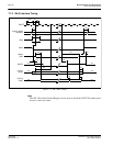
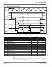
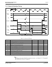
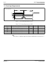
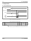
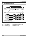
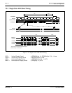
7.3.1 Power On/Reset Timing
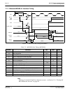
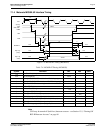
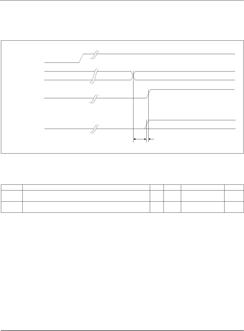
Figure 7-9: LCD Panel Power On/Reset Timing
Note
Where T
FPFRAME
is the period of FPFRAME and T
PCLK
is the period of the pixel clock.
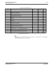
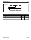
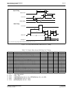
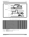
Table 7-9: LCD Panel Power On/Reset Timing
Symbol Parameter Min Typ Max Units
t1
REG[03h] to FPLINE, FPFRAME, FPSHIFT, FPDAT, DRDY
active
T
FPFRAME
ns
t2
FPLINE, FPFRAME, FPSHIFT, FPDAT, DRDY active to
LCDPWR
0Frames
RESET#
REG[03h] bits [1:0]
LCDPWR
FPLINE
FPSHIFT
FPDAT
DRDY
t1
t2
00 11
FPFRAME
ACTIVE


