


Page 66 Epson Research and Development
Vancouver Design Center
S1D13705 Hardware Functional Specification
X27A-A-001-10 Issue Date: 02/02/01
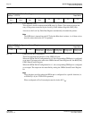
bits 7-4 LUT Data Bits [3:0]
This register is used to read/write the RGB Look-Up Tables. This register accesses the
entry at the pointer controlled by the Look-Up Table Address Register (REG[15h]).
Accesses to the Look-Up Table Data Register automatically increment the pointer.
Note
The RGB data is inserted into the LUT after the Blue data is written, i.e. all three colors
must be written before the LUT is updated.
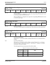
bits 4-0 GPIO[4:0] Pin IO Configuration
These bits determine the direction of the GPIO[4:0] pins.
When the GPIOn Pin IO Configuration bit = 0, the corresponding GPIOn pin is configured
as an input. The input can be read at the GPIOn Status/Control Register bit. See REG[19h]
GPIO Status/Control Register.
When the GPIOn Pin IO Configuration bit = 1, the corresponding GPIOn pin is configured
as an output. The output can be controlled by writing the GPIOn Status/Control Register
bit.
Note
These bits have no effect when the GPIOn pin is configured for a specific function (i.e.
as FPDAT[11:8] for TFT/D-TFD operation).
When configured as IO, all unused pins must be tied to IO V
DD
.
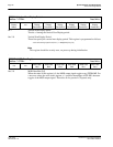
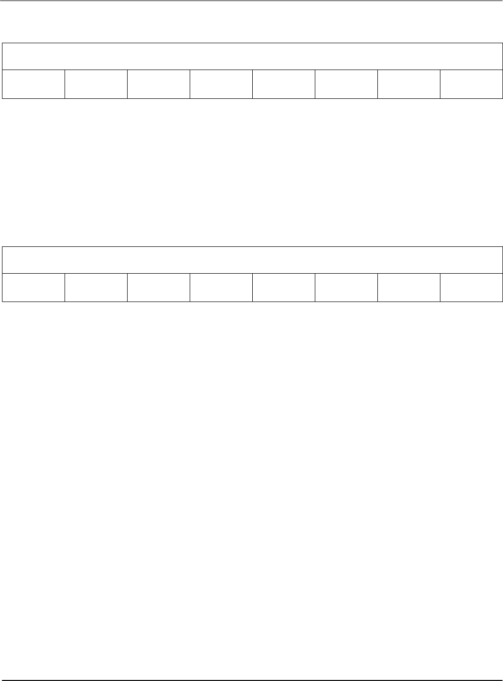
REG[17h] Look-Up Table Data Register
Address = 1FFF7h Read/Write
LUT Data
Bit 3
LUT Data
Bit 2
LUT Data
Bit 1
LUT Data
Bit 0
n/a n/a n/a n/a
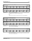
REG[18h] GPIO Configuration Control Register
Address = 1FFF8h Read/Write
n/a n/a n/a
GPIO4 Pin IO
Configuration
GPIO3 Pin IO
Configuration
GPIO2 Pin IO
Configuration
GPIO1 Pin IO
Configuration
GPIO0 Pin IO
Configuration