Epson Research and Development Page 19
Vancouver Design Center
Hardware Functional Specification S1D13705
Issue Date: 02/02/01 X27A-A-001-10
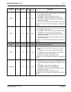
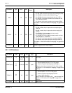
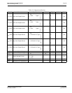
WE0# I 77 CS Input
This pin has multiple functions.
• For SH-3/SH-4 mode, this pin inputs the write enable signal
for the lower data byte (WE0#).
• For MC68K #1, this pin must be tied to IO V
DD
• For MC68K #2, this pin inputs the bus size bit 0 (SIZ0).
• For Generic #1, this pin inputs the write enable signal for the
lower data byte (WE0#).
• For Generic #2, this pin inputs the write enable signal (WE#)
See Table 5-2: “Host Bus Interface Pin Mapping,” on page 22
for
summary.
WE1# I 78 CS Input
This pin has multiple functions.
• For SH-3/SH-4 mode, this pin inputs the write enable signal
for the upper data byte (WE1#).
• For MC68K #1, this pin inputs the upper data strobe (UDS#).
• For MC68K #2, this pin inputs the data strobe (DS#).
• For Generic #1, this pin inputs the write enable signal for the
upper data byte (WE1#).
• For Generic #2, this pin inputs the byte enable signal for the
high data byte (BHE#).
See Table 5-2: “Host Bus Interface Pin Mapping,” on page 22
for
summary.
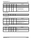
CS# I 74 C Input This pin inputs the chip select signal.
BCLK I 71 C Input This pin inputs the system bus clock.
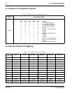
BS# I 75 CS Input
This pin has multiple functions.
• For SH-3/SH-4 mode, this pin inputs the bus start signal
(BS#).
• For MC68K #1, this pin inputs the address strobe (AS#).
• For MC68K #2, this pin inputs the address strobe (AS#).
• For Generic #1, this pin must be tied to V
SS
.
• For Generic #2, this pin must be tied to IO V
DD
.
See Table 5-2: “Host Bus Interface Pin Mapping,” on page 22
for
summary.
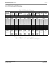
RD/WR# I 79 CS Input
This pin has multiple functions.
• For SH-3/SH-4 mode, this pin inputs the RD/WR# signal.
The S1D13705 needs this signal for early decode of the bus
cycle.
• For MC68K #1, this pin inputs the R/W# signal.
• For MC68K #2, this pin inputs the R/W# signal.
• For Generic #1, this pin inputs the read command for the
upper data byte (RD1#).
• For Generic #2, this pin must be tied to IO V
DD
.
See Table 5-2: “Host Bus Interface Pin Mapping,” on page 22
for
summary.
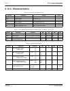
Pin NamesTypePin #Cell
RESET#
State
Description


