


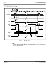
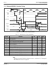
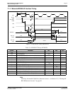
Page 24 Epson Research and Development
Vancouver Design Center
S1D13705 Hardware Functional Specification
X27A-A-001-10 Issue Date: 02/02/01
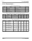
6 D.C. Characteristics
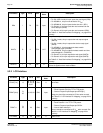
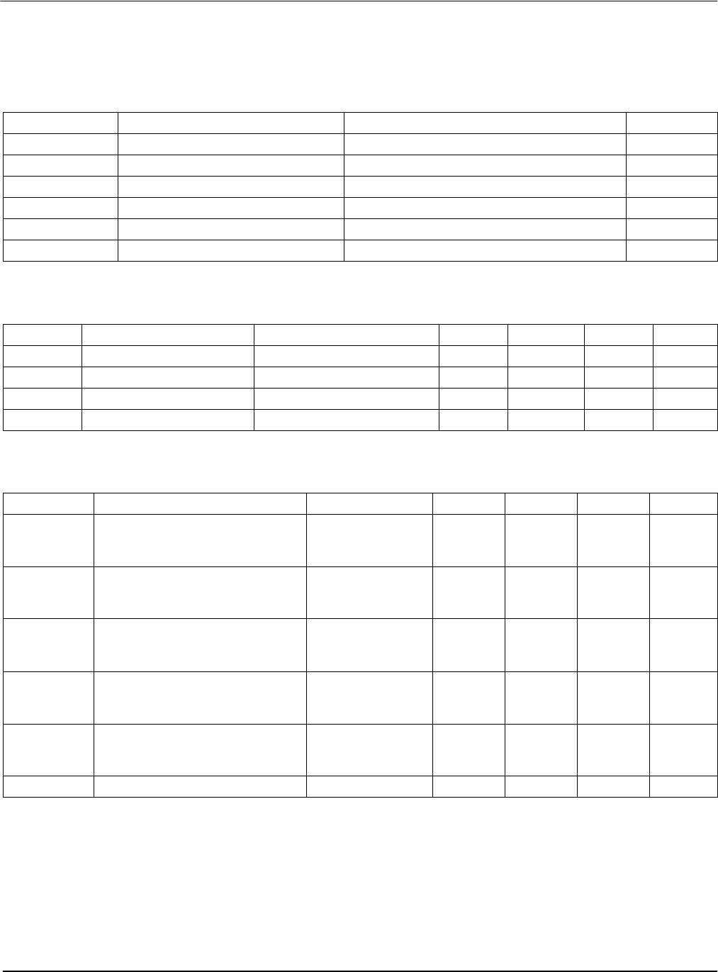
Table 6-1: Absolute Maximum Ratings
Symbol Parameter Rating Units
Core V
DD
Supply Voltage V
SS
- 0.3 to 4.0 V
IO V
DD
Supply Voltage Core V
DD
to 7.0 V
V
IN
Input Voltage V
SS
- 0.3 to IO V
DD
+ 0.5 V
V
OUT
Output Voltage V
SS
- 0.3 to IO V
DD
+ 0.5 V
T
STG
Storage Temperature -65 to 150 ° C
T
SOL
Solder Temperature/Time 260 for 10 sec. max at lead ° C
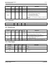
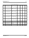
Table 6-2: Recommended Operating Conditions for Core VDD = 3.3V ± 10%
Symbol Parameter Condition Min Typ Max Units
Core V
DD
Supply Voltage V
SS
= 0 V 2.7 3.0/3.3 3.6 V
IO V
DD
Supply Voltage V
SS
= 0 V, IO V
DD
≥ Core V
DD
2.7 3.0/3.3/5.0 5.5 V
V
IN
Input Voltage V
SS
IO V
DD
V
T
OPR
Operating Temperature -40 25 85 ° C
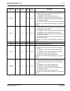
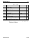
Table 6-3: Input Specifications
Symbol Parameter Condition Min Typ Max Units
V
IL
Low Level Input Voltage
CMOS inputs
IO V
DD
= 3.0
3.3
5.0
0.8
0.8
1.0
V
V
IH
High Level Input Voltage
CMOS inputs
IO V
DD
= 3.0
3.3
5.0
1.9
2.0
3.5
V
V
T+
Positive-going Threshold
CMOS Schmitt inputs
IO V
DD
= 3.0
3.3
5.0
1.0
1.1
2.0
2.3
2.4
4.0
V
V
T-
Negative-going Threshold
CMOS Schmitt inputs
IO V
DD
= 3.0
3.3
5.0
0.5
0.6
0.8
1.7
1.8
3.1
V
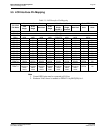
I
IZ
Input Leakage Current
V
DD
= Max
V
IH
= V
DD
V
IL
= V
SS
-1 1 µA
C
IN
Input Pin Capacitance 10 pF