


IXF1104 Quad-Port 10/100/1000 Mbps Ethernet Media Access Controller
110 Datasheet
Document Number: 278757
Revision Number: 007
Revision Date: March 25, 2004
b. Initiate the I
2
C transfer by setting bit [24] of the control register to 0x1.
c. Select the port by using bits [17:16].
d. Select the Read mode of operation by setting bit [15] to 0x1.
e. Select the Device ID by setting bits [14:11].
f. Select the register address by setting bits [10:0].
2. Set the Device ID field to 0xA and the register address (bits 10:8) to 0x0 to access the fiber
module serial E2PROM. Setting the Device ID field to 0xA and the Register Address [10:8] to
0x0 permits read-only access.
3. Set the Device ID field to 0xA and the Register Address [10:8] between the values of 0x1 and
0x7 to access the PHY registers.
4. Poll the Read_Valid field, bit 20. The read data is available when this bit is set to 0x1.
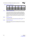
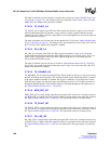
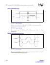
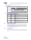
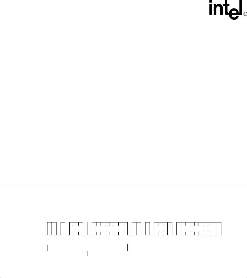
Figure 24 shows an 8-bit read access.
Note: The user software ensures the order of the contiguous accesses required to read the High and Low
bytes of 16-bit-wide PHY registers.
Note: Only one optical module I²C access sequence can be run at any given time. If a second write is
carried out to the “I2C Control Ports 0 - 3 ($0x79B)" and “I2C Data Ports 0 - 3 ($0x79F)" before a
result is returned for the previous write, the data for the first write is lost. An internal state machine
completes the Optical Module Interface register access for the first write. It attempts to place the
data in the DataRead field and checks to see if the WriteCommand bit is 00h. If it is not 00h, it
discards the data and signals the I²C access state machine to begin a new cycle using the data from
the second write.
5.7.3.3 I
2
C Write Operation
The following sequence provides an example of writing data to Register Address 0xFF for Port 3:
1. Program the “I2C Control Ports 0 - 3 ($0x79B)" with the following information:
a. Enable the I
2
C block by setting Register bit 25 to 0x1.
b. Set the port to be accessed by setting Register bits 17:16 to 0x3.
c. Select a Write access by setting Register bit 15 to 0x0.
Figure 24. I
2
C Random Read Transaction
DEVICE
ADDRESS
DEVICE
A DDRE SS
WORD
A DDR ESS
I
2
C_Data Line
DUMMY WRI TE
(* = DON' T CARE bi t for 1k)
START
S
T
A
R
T
R
E
A
D
S
T
A
R
T
W
R
I
T
E
S
T
O
P
M
S
B
M
S
B
M
S
B
L
S
B
R
/
W
L
S
B
DAT A n
L
S
B
A
C
K
N
O
A
C
K
A
C
K
*