


IXF1104 4-Port Gigabit Ethernet Media Access Controller
Datasheet 43
Document Number: 278757
Revision Number: 007
Revision Date: March 25, 2004
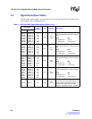
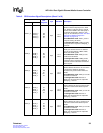
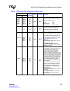
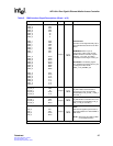
RDAT7
RDAT6
RDAT5
RDAT4
RDAT3
RDAT2
RDAT1
RDAT0
RDAT7_0
RDAT6_0
RDAT5_0
RDAT4_0
RDAT3_0
RDAT2_0
RDAT1_0
RDAT0_0
F14
E14
D14
C13
C14
B14
A14
A15
Output
3.3 V
LVTTL
Receive Data Bus.
RDAT carries payload data and in-band
addresses from the IXF1104.
Mode
32-bit Multi-PHY
4 x 8 Single-PHY
Bits
[7:0]
[7:0] for port 0
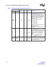
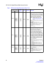
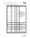
RFCLK RFCLK A19 Input
3.3 V
LVTTL
Receive Clock.
RFCLK is the clock associated with all
receive signals. Data and controls are
driven on the rising edge of RFCLK
(frequency operation range 90 - 133 MHz).
RPRTY_0 RPRTY_0
RPRTY_1
RPRTY_2
RPRTY_3
E15
G16
E20
F20
Output
3.3 V
LVTTL
Receive Parity.
RPRTY indicates odd parity for the RDAT
bus. RPRTY is valid only when a channel
asserts RENB or RSX. Odd parity is the
default configuration; however, even parity
can be selected (see Table 147 on
page 214).
32-bit Multi-PHY mode: RPRTY_0 is the
parity bit for all 32 bits.
4 x 8 Single-PHY mode: Each bit of
RPRTY_0:3 corresponds to the respective
RDAT[3:0]_n channel.
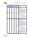
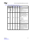
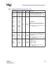
RENB_0 RENB_0
RENB_1
RENB_2
RENB_3
A13
A18
C19
E24
Input
3.3 V
LVTTL
Receive Read Enable.
The RENB signal controls the flow of data
from the receive FIFOs. During data
transfer, RVAL must be monitored as it
indicates if the RDAT[31:0], RPRTY,
RMOD[1:0], RSOP, REOP, RERR, and RSX
are valid. The system may de-assert RENB
at any time if it is unable to accept data from
the IXF1104. When RENB is sampled Low,
a read is performed from the receive FIFO
and the RDAT[31:0], RPRTY, RMOD[1:0],
RSOP, REOP, RERR, RSX and RVAL
signals are updated on the following rising
edge of RFCLK.
When RENB is sampled High by the PHY
device, a read is not performed, and the
RDAT[31:0], RPRTY, RMOD[1:0], RSOP,
REOP, RERR, RSX, and RVAL signals
remain unchanged on the following rising
edge of RFCLK.
32-bit Multi-PHY Mode: RENB_0 covers all
receive bits.
4 x 8 Single-PHY Mode: The RENB_0:3
bits correspond to the per-port data and
control signals.
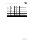
Table 3. SPI3 Interface Signal Descriptions (Sheet 6 of 8)
Signal Name
Ball
Designator
Type Standard Description
MPHY SPHY