


IXF1104 Quad-Port 10/100/1000 Mbps Ethernet Media Access Controller
116 Datasheet
Document Number: 278757
Revision Number: 007
Revision Date: March 25, 2004
When implemented on the board with the M5450 device, the LED DATA bit 1 appears on Output
bit 3 of the M5450 and the LED DATA bit 2 appears on Output bit 4, etc. This means that Output
bits 1, 2, and 15 through 35 will never have valid data and should not be used.
5.8.4 Mode 1: Detailed Operation
Note: Please refer to generic specifications for 74LS/HC599 for information on device operation.
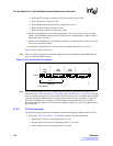
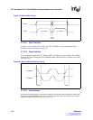
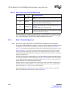
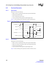
The operation of the LED Interface in Mode 1 is based on a 36-bit counter loop. The data for each
LED is placed in turn on the serial data line and clocked out by the LED_CLK. Figure 30 on
page 117 shows the basic timing relationship and relative positioning in the data stream of each bit.
Figure 30 on page 117 shows the 36 clocks which are output on the LED_CLK pin. The data is
changed on the falling edge of the clock and is valid for the almost the entire clock cycle. This
ensures that the data is valid during the rising edge of the LED_CLK, which clocks the data into the
shift register chain devices.
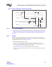
The LED_LATCH signal is required in Mode 1, and latches the data shifted into the shift register
chain into the output latches of the 74HC599 device. Figure 30 shows that the LED_LATCH signal
is active High during the Low period on the 35th LED_CLK cycle. This avoids any possibility of
trying to latch data as it is shifting through the register.
When this operation mode is implemented on a board with a shift register chain containing three
74HC599 devices, the LED DATA bit 1 is output on Shift register bit 1, and so on up the chain.
Only Shift register bits 31 and 32 do not contain valid data.
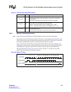
The actual data shown in Figure 30 consists of a 36-bit chain, of which 12 bits are valid LED
DATA. The 36-bit data chain is built up as shown in Figure 30.
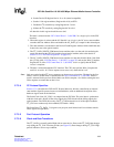
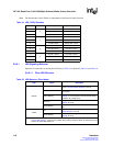
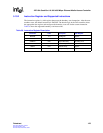
Table 32. Mode 0 Clock Cycle to Data Bit Relationship
LED_CLK Cycle
LED_DATA
Name
LED_DATA Description
1START BIT
This bit synchronizes the M5450 device to expect 35 bits of data to
follow.
2:3 PAD BITS
These bits are used only as fillers in the data stream to extend the
length from the actual 12-bit LED DATA to the required 18-bit frame
length. These bits should always be a logic 0.
4:15 LED DATA 1-12
These bits are the actual data transmitted to the M5450 device. The
decode for each individual bit in each mode is defined in Table 34 on
page 118.
The data is TRUE. Logic 1 (LED ON) = High
36:38 PAD BITS
These bits are used as fillers in the data stream to extend the length
from the actual 30-bit LED DATA to the required 36-bit frame length.
These bits should always be a logic 0.