


IXF1104 4-Port Gigabit Ethernet Media Access Controller
36 Datasheet
Document Number: 278757
Revision Number: 007
Revision Date: March 25, 2004
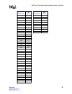
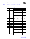
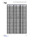
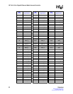
4.0 Ball Assignments and Signal Descriptions
4.1 Naming Conventions
4.1.1 Signal Name Conventions
Signal names begin with a Signal Mnemonic, and can also contain one or more of the following
designations: a differential pair designation, a serial designation, a port designation (RGMII
interface), and an active low designation. Signal naming conventions are as follows:
Differential Pair + Port Designation. The positive and negative components of differential pairs
tied to a specific port are designated by the Signal Mnemonic, immediately followed by an
underscore and either P (positive component) or N (negative component), and an underscore
followed by the port designation. For example, SerDes interface signals for port 0 are identified as
TX_P_0 and TX_N_0.
Serial Designation. A set of signals that are not tied to any specific port are designated by the
Signal Mnemonic, followed by a bracketed serial designation. For example, the set of 11 CPU
Address Bus signals is identified as UPX_ADD[10:0].
Port Designation. Individual signals that apply to a particular port are designated by the Signal
Mnemonic, immediately followed by an underscore and the Port Designation. For example,
RGMII Transmit Control signals are identified as TX_CTL_0, TX_CTL_1, TX_CTL_2, and so on.
Port Bus Designation. A set of bus signals that apply to a particular port are designated by the
Signal Mnemonic, immediately followed by a bracketed bus designation, followed by an
underscore and the port designation. For example, RGMII transmit data bus signals are identified
as TD[3:0]_0, TD[3:0]_1, TD[3:0]_2, and so on.
Active Low Designation. A control input or indicator output that is active Low is designated by a
final suffix consisting of an underscore followed by an upper case “L”. For example, the CPU cycle
complete identifier is shown as UPX_RDY_L.
4.1.2 Register Address Conventions
Registers located in on-chip memory are accessed using a register address, which is provided in
Hex notation. A Register Address is indicated by the dollar sign ($), followed by the memory
location in Hex.