


IXF1104 Quad-Port 10/100/1000 Mbps Ethernet Media Access Controller
Datasheet 113
Document Number: 278757
Revision Number: 007
Revision Date: March 25, 2004
5.7.3.6.4 Memory Reset
After an interruption in protocol, power loss, or system reset, any 2-wire optical module can be
reset by following three steps:
1. Clock up to 9 cycles
2. Wait for I
2
C_DATA High in each cycle while I
2
C_CLK is High
3. Initiate a start condition.
5.7.3.6.5 Device Addressing
All E²PROMs in SFP optical module devices require an 8-bit device address word following a start
condition to enable the chip to read or write. The device address word consists of a mandatory one,
zero sequence for the four most-significant bits. This is common to all devices. The next three bits
are the A2, A1, and A0 device address bits that are tied to zero in an optical module. The eighth bit
of the device address is the Read/Write operation select bit. A Read operation is initiated if this bit
is High and a Write operation is initiated if this bit is Low.
Upon comparison of the device address, the optical module outputs a zero. If a comparison is not
made, the optical module E²PROM returns to a standby state.
5.7.3.6.6 Random Read Operation
A random Read requires a “dummy” Byte/Write sequence to load the data word address. The
“dummy” write is achieved by first sending the device address word with the Read/Write bit
cleared to Low, which signals a Write operation. The optical module acknowledges receipt of the
device address word. The IXF1104 sends the data word address, which is again acknowledged by
the optical module. The IXF1104 generates another start condition. This completes the “dummy”
write and sets the optical module E²PROM pointers to the desired location.
The IXF1104 initiates a current address read by sending a device address with the Read/Write bit
set High. The optical module acknowledges the device address and serially clocks out the data
word. The IXF1104 does not respond with a zero but generates a stop condition (see Figure 28).
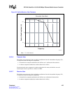
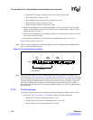
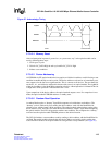
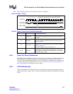
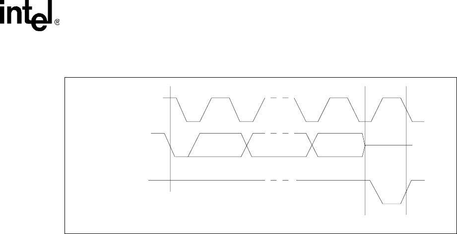
Figure 27. Acknowledge Timing
START ACKNOWLEDGE
I
2
C_Data
DATA IN
DATA OUT