


IXF1104 4-Port Gigabit Ethernet Media Access Controller
38 Datasheet
Document Number: 278757
Revision Number: 007
Revision Date: March 25, 2004
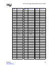
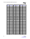
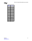
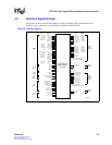
4.3 Signal Description Tables
The I/O signals, power supplies, or ground returns associated with each IXF1104 connection ball
are described in Table 3 through Table 14.
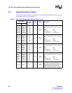
Table 3. SPI3 Interface Signal Descriptions (Sheet 1 of 8)
Signal Name
Ball
Designator
Type Standard Description
MPHY SPHY
TDAT31
TDAT30
TDAT29
TDAT28
TDAT27
TDAT26
TDAT25
TDAT24
TDAT7_3
TDAT6_3
TDAT5_3
TDAT4_3
TDAT3_3
TDAT2_3
TDAT1_3
TDAT0_3
F7
F5
G9
G8
G7
G6
G5
G4
Input
3.3 V
LVTTL
Transmit Data Bus.
Carries payload data to the IXF1104 egress
path.
Mode
32-bit Multi-PHY
4 x 8 Single-PHY
Bits
[31:24]
[7:0] for port 3
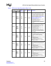
TDAT23
TDAT22
TDAT21
TDAT20
TDAT19
TDAT18
TDAT17
TDAT16
TDAT7_2
TDAT6_2
TDAT5_2
TDAT4_2
TDAT3_2
TDAT2_2
TDAT1_2
TDAT0_2
C8
F9
E10
E9
E8
E7
E6
E5
Input
3.3 V
LVTTL
Transmit Data Bus.
Carries payload data to the IXF1104 egress
path.
Mode
32-bit Multi-PHY
4 x 8 Single-PHY
Bits
[23:16]
[7:0] for port 2
TDAT15
TDAT14
TDAT13
TDAT12
TDAT11
TDAT10
TDAT9
TDAT8
TDAT7_1
TDAT6_1
TDAT5_1
TDAT4_1
TDAT3_1
TDAT2_1
TDAT1_1
TDAT0_1
H3
J3
J2
J1
H1
G2
G1
F1
Input
3.3 V
LVTTL
Transmit Data Bus.
Carries payload data to the IXF1104 egress
path.
Mode
32-bit Multi-PHY
4 x 8 Single-PHY
Bits
[15:8]
[7:0] for port 1
TDAT7
TDAT6
TDAT5
TDAT4
TDAT3
TDAT2
TDAT1
TDAT0
TDAT7_0
TDAT6_0
TDAT5_0
TDAT4_0
TDAT3_0
TDAT2_0
TDAT1_0
TDAT0_0
C6
B5
C5
C4
D1
C3
C2
B3
Input
3.3 V
LVTTL
Transmit Data Bus.
Carries payload data to the IXF1104 egress
path.
Mode
32-bit Multi-PHY
4 x 8 Single-PHY
Bits
7:0]
[7:0] for port 0
TFCLK TFCLK D7 Input
3.3 V
LVTTL
Transmit Clock.
TFCLK is the clock associated with all
transmit signals. Data and control lines are
sampled on the rising edge of TFCLK
(frequency operation range 90 - 133 MHz).