


IXF1104 Quad-Port 10/100/1000 Mbps Ethernet Media Access Controller
Datasheet 111
Document Number: 278757
Revision Number: 007
Revision Date: March 25, 2004
d. Set the Device ID Register bits 14:11 to Ah (Atmel compatible).
e. Set the 11-bit register address (Register bits 10:0) to 0FFh.
f. Enable the I
2
C controller by setting Register bit 2 to 0x1.
g. Initiate the I
2
C transfer by setting Register bit 24 to 0x1.
All other bits in this register should be set to 0x0.
This data is written into the “I2C Control Ports 0 - 3 ($0x79B)" in a single cycle via the CPU
interface.
2. When this register is written and the I
2
C Start bit is at a Logic 1, the I
2
C access state machine
examines the Port Address Select and enables the I
2
C_DATA_0:3 output for the selected port.
3. The state machines uses the data in the Device ID and Register Address fields to build the data
frame to be sent to the optical module
4. The I
2
C_DATA_WRITE_FSM internal state machine takes over the task of transferring the
actual data between the IXF1104 and the selected optical module (refer to the details in
Section 5.7.3.4, “I²C Protocol Specifics” on page 111).
5. The I
2
C_DATA_WRITE_FSM internal state machine uses the data from the Write_Data field
bits [23:16] of the “I2C Data Ports 0 - 3 ($0x79F)” on page 222 and sets the Write_Complete
Register bit 22 of the “I2C Control Ports 0 - 3 ($0x79B)" to 0x1 to signify that the Write
Access is complete.
6. The data is written through the CPU interface. The CPU must poll the Write_Complete bit
until it is set to 0x1. It is safe to request a new access only when this bit is set.
Note: Only one optical module I
2
C access sequence can be run at any given time. The data for the first
Write is lost if a second Write is carried out to the “I2C Control Ports 0 - 3 ($0x79B)" before a
result is returned for the previous Write. Make sure Write complete = 0x1 before starting the next
Write sequence to ensure that no data is lost.
5.7.3.4 I²C Protocol Specifics
Section 5.7.3.4 describes the IXF1104 I²C Protocol behavior, which is controlled by an internal
state machine. Specific protocol states are defined below, with an additional description of the
hardware signals used on the interface.
The Serial Clock Line (I
2
C_CLK) is an output from the IXF1104. The serial data is synchronous
with this clock and is driven off the rising edge by the IXF1104 and off the falling edge by the
optical module. The IXF1104 has only one I
2
C_CLK line that drives all of the optical modules.
I
2
C_CLK runs continuously when enabled (I²C Enable = 01h0).
The Serial Data (I
2
C_DATA_3:0) signals (one per port) are bi-directional for serial data transfer.
These signals are open drain.
5.7.3.5 Port Protocol Operation
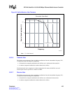
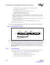
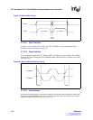
5.7.3.6 Clock and Data Transitions
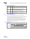
The I
2
C_DATA is normally pulled High with an extra device. Data on the I
2
C_DATA pin changes
only during the I
2
C_CLK Low time periods (see Figure 25). Data changes during I
2
C_CLK High
periods indicate a start or stop condition.