


IXF1104 Quad-Port 10/100/1000 Mbps Ethernet Media Access Controller
124 Datasheet
Document Number: 278757
Revision Number: 007
Revision Date: March 25, 2004
5.10.3 ID Register
The ID register is a 32-bit register. The IDCODE instruction connects this register between TDI
and TDO. See Table 112 “JTAG ID ($0x50C)” on page 191 for detailed information.
5.10.4 Boundary Scan Register
The Boundary Scan register is a shift register made up of all the boundary scan cells associated
with the device signals. The number, type, and order of the boundary scan cells are specified in the
IXF1104 BSDL file. The EXTEST and SAMPLE instructions connect this register between TDI
and TDO.
5.10.5 Bypass Register
The Bypass register is a 1-bit register that bypasses the IXF1104 to reduce the JTAG chain length
when accessing other devices on the chain besides the IXF1104. The BYPASS, HIGHZ, and
CLAMP instructions connect this register between TDI and TDO.
5.11 Loopback Modes
The IXF1104 provides two loopback modes for device diagnostic testing when it has been
integrated into a user system. A line-side loopback allows the line-side receive interface to be
looped back to the transmit line-side interface. A SPI3 loopback mode allows the SPI3 transmit
interface to be looped back to the SPI3 receive interface.
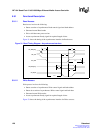
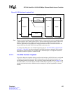
5.11.1 SPI3 Interface Loopback
To provide a diagnostic loopback feature on the SPI3 interface, it is possible to configure the
IXF1104 to loop back any data written to the IXF1104 through the SPI3 transmit interface back to
the SPI3 receive interface. This is accomplished using the data path shown in Figure 33.
Note: Loopback packets also appear on the line side TX interface.