Contents
12 Datasheet
Document Number: 278757
Revision Number: 007
Revision Date: March 25, 2004
Revision History
Revision Number: 007
Revision Date: March 25, 2004
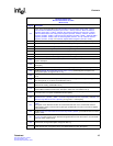
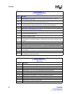
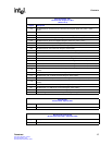
(Sheet 1 of 5)
Page # Description
All Globally replaced GBIC with Optical Module Interface.
All Globally edited signal names.
All
Globally changed SerDes and PLL analog power ball names as follows:
TXAVTT and RXAVTT changed to AVDD1P8_2
TXAV25 and RXAV25 changed to AVDD2P5_2
PLL1_VDDA and PLL2_VDDA changed to AVDD1P8_1
PLL3_VDDA changed to AVDD2P5_1
PLL1_GNDA, PLL2_GNDA, and PLL3_GNDA changed to GND
1
Reworded and rearranged the Product Features section on page one
Changed Jumbo frame support from “10 kbytes” to “9.6 KB”.
20 Changed heading to Section 2.0, “General Description” [was Section 2.0, “Block Diagram”].
22/36
Reversed sections as follows:
Section 3.0, “Ball Assignments and Ball List Tables”
Section 4.0, “Ball Assignments and Signal Descriptions”
23
Modified Table 1 “Ball List in Alphanumeric Order by Signal Name”:
Changed A10 from VCC to VDD
Changed C12 from VCC to VDD
Changed D11 from VCC to VDD
Changed J20 from GND to VDD
Changed Ball A1 from NC to No Pad.
Changed Balls A2, A3, A22, A23, A24, B1, B2, B23, B24, C1, C24, AB1, AB24, AC1, AC2, AC23,
AC24, AD1, AD2, AD3, AD22, AD23, AD24 from NC to No Ball.
29
Modified Table 2 “Ball List in Alphanumeric Order by Ball Location”
Changed A10 from VCC to VDD
Changed C12 form VCC to VDD
Changed D11 from VCC to VDD
Changed J20 from GND to VDD
Changed Ball A1 from NC to No Pad.
Changed Balls A2, A3, A22, A23, A24, B1, B2, B23, B24, C1, C24, AB1, AB24, AC1, AC2, AC23,
AC24, AD1, AD2, AD3, AD22, AD23, AD24 from NC to No Ball.
37
Updated Figure 4 “Interface Signals” [modified SPI3 interface signals and added MPHY and SPHY
categories; modified signal names].
38
Broke old Table 1, “IXF1104 Signal Descriptions” into the following:
Table 3 “SPI3 Interface Signal Descriptions” on page 38 through Table 14 “Power Supply Signal
Descriptions” on page 55
38
Modified Table 3 “SPI3 Interface Signal Descriptions” on page 38 [edited description for DTPA;
added text to TFCLK description; added text to RFCLK description].
49
Modified Table 6 “RGMII Interface Signal Descriptions” [Added Ball Designators; added notes
under descriptions].
50 Modified Table 7 “CPU Interface Signal Descriptions” [UPX_DATA[16]: deleted J10, added M10].
52 Modified Table 9 “Optical Module Interface Signal Descriptions” [added Ball Designators].
53 Modified Table 10 “MDIO Interface Signal Descriptions” [moved note from MDC to MDIO].
55
Modified Table 14 “Power Supply Signal Descriptions” [added Ball Designators A4, A21, and AD21
to GND; added AVDD1P8_1, AVDD1P8_2, AVDD2P5_1, and AVDD2P5_2].


