


IXF1104 4-Port Gigabit Ethernet Media Access Controller
Datasheet 63
Document Number: 278757
Revision Number: 007
Revision Date: March 25, 2004
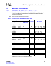
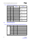
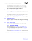
4.8 Pull-Up/Pull-Down Ball Guidelines
The signals shown in Table 20 require the addition of a pull-up or pull-down resistor to the board
design for normal operation. Any balls marked as unused (NC) should be unconnected.
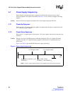
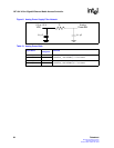
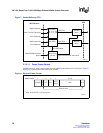
4.9 Analog Power Filtering
Figure 21 illustrates an analog power supply filter network and Table 21 lists the analog power
balls.
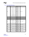
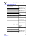
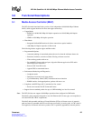
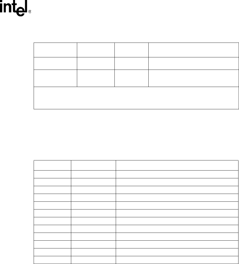
Table 19. Power Supply Sequencing
Power Supply Power-Up Order
Time Delta to
Next Supply
1
Notes
VDD, AVDD1P8_1,
AVDD1P8_2
First 0 1.8 V supplies
VDD4, VDD5,
AVDD2P5_1,
AVDD2P5_2
Second 10 µs 2.5 V supplies
1. The value of 10 µs given is a nominal value only. The exact time difference between the application of the 2.5 V analog
supply is determined by a number of factors, depending on the power management method used. To avoid damage to the
IXF1104, the TXAV25 supply must not exceed the VDD supply by more than 2 V at any time during the power-up or
power-down sequence.
NOTE: The 3.3 V supply (VDD2 and VDD3) can be applied at any point during this sequence.
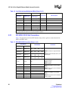
Table 20. Pull-Up/Pull-Down and Unused Ball Guidelines
Pin Name Pull-Up/Pull-Down Comments
TX_FAULT_INT Pull-up 4.7 k Ω to 2.5 V. Optical module signal with open-drain I/O.
RX_LOS_INT Pull-up 4.7 k Ω to 2.5 V. Optical module signal with open-drain I/O.
MOD_DEF_INT Pull-up 4.7 k Ω to 2.5 V. Optical module signal with open-drain I/O.
TDI Pull-up 10 k Ω to 3.3 V. JTAG test pin.
TDO Pull-up 10 k Ω to 3.3 V. JTAG test pin.
TMS Pull-up 10 k Ω to 3.3 V. JTAG test pin.
TCLK Pull-up 10 k Ω to 3.3 V. JTAG test pin.
TRST_L Pull-down 10 k Ω to 3.3 V. JTAG test pin.
MDIO Pull-up 4.7 k Ω to 2.5 V
UPX_RDY_L Pull-up 4.7 k Ω to 3.3 V
I
2
C_DATA_0:3 Pull-up 4.7 k Ω to 2.5 V
TX_DISABLE_0:3 Pull-up 4.7 k Ω to 2.5 V