


IXF1104 4-Port Gigabit Ethernet Media Access Controller
Datasheet 49
Document Number: 278757
Revision Number: 007
Revision Date: March 25, 2004
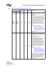
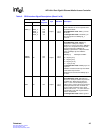
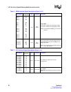
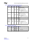
Table 6. RGMII Interface Signal Descriptions (Sheet 1 of 2)
Signal Name
Ball
Designator
Type Standard Description
TXC_0
TXC_1
TXC_2
TXC_3
AA1
AD7
AC20
AB14
Output
2.5 V
CMOS
Source Synchronous Transmit Clock.
This clock is supplied synchronous to the transmit
data bus in either RGMII or GMII mode.
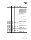
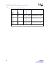
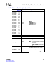
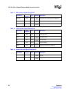
TD3_0
TD2_0
TD1_0
TD0_0
TD3_1
TD2_1
TD1_1
TD0_1
TD3_2
TD2_2
TD1_2
TD0_2
TD3_3
TD2_3
TD1_3
TD0_3
AA3
Y3
Y2
Y1
AD9
AB9
AB7
AC7
AB23
AB22
AB21
AB20
V17
V16
V15
V14
Output
2.5 V
CMOS
Transmit Data.
Bits [3:0] are clocked on the rising edge of TXC.
Bits [7:4] are clocked on the falling edge of TXC.
NOTE: Shares data signals TXD[3:0]_n with the
GMII interface.
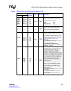
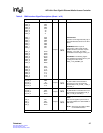
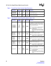
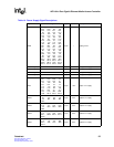
TX_CTL_0
TX_CTL_1
TX_CTL_2
TX_CTL_3
AB2
Y8
AC22
V12
Output
2.5 V
CMOS
Transmit Control.
TX_CTL is TX_EN on the rising edge of TXC and a
logical derivative of TX_EN and TX_ER on the
falling edge of TXC.
NOTE: TX_CTL multiplexes with TX_EN_n on the
GMII interface.
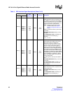
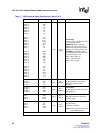
RXC_0
RXC_1
RXC_2
RXC_3
V4
AD11
AA24
V23
Input
2.5 V
CMOS
Receiver Reference Clock.
Operates at:
125 MHz for 1 Gigabit
25 MHz for 100 Mbps
2.5 MHz for 10 Mbps
NOTE: Shares the same balls as RXC on the
GMII interface.