


113
CHAPTER 5 CPU ARCHITECTURE
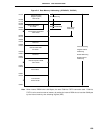
5.2.2 General registers
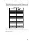
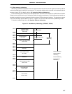
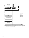
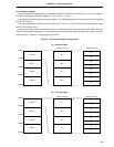
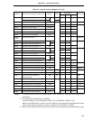
A general register is mapped at particular addresses (FEE0H to FEFFH) of the data memory. It consists of 4 banks,
each bank consisting of eight 8-bit registers (X, A, C, B, E, D, L, and H).
Each register can also be used as an 8-bit register. Two 8-bit registers can be used in pairs as a 16-bit register
(AX, BC, DE, and HL).
They can be described in terms of function names (X, A, C, B, E, D, L, H, AX, BC, DE, and HL) and absolute names
(R0 to R7 and RP0 to RP3).
Register banks to be used for instruction execution are set with the CPU control instruction (SEL RBn). Because
of the 4-register bank configuration, an efficient program can be created by switching between a register for normal
processing and a register for interruption for each bank.
Figure 5-12. General Register Configuration
(a) Absolute Name
(b) Function Name
BANK0
BANK1
BANK2
BANK3
FEFFH
FEF8H
FEE0H
RP3
RP2
RP1
RP0
R7
15 0 7 0
R6
R5
R4
R3
R2
R1
R0
16-Bit Processing 8-Bit Processing
FEE0H
FEE8H
BANK0
BANK1
BANK2
BANK3
FEFFH
FEF8H
FEE0H
HL
DE
BC
AX
H
15 0 7 0
L
D
E
B
C
A
X
16-Bit Processing 8-Bit Processing
FEF0H
FEE8H