


411
CHAPTER 18 SERIAL INTERFACE CHANNEL 0 (
µ
PD78078Y Subseries)
18.4.6 Restrictions in I
2
C bus mode
The following restrictions apply to the
µ
PD78078Y Subseries.
• Restrictions when used as slave device in I
2
C bus mode
Applicable models
µ
PD78076Y, 78078Y, 78P078Y, and IE-78078-R-EM
Description When the wake-up function is executed (by setting the WUP flag (bit 5 of the serial
operation mode register 0 (CSIM0)) in the serial transfer status
Note
, data between the
other slaves and master will be judged as an address. If this data happens to coincide
with the slave address of the
µ
PD78078Y Subseries, the
µ
PD78078Y Subseries will
initiate communication, destroying the communication data.
Note The serial transfer status is the status in which the interrupt request flag (CSIIF0)
is set because of the end of serial transfer after the serial I/O shift register 0
(SIO0) has been written.
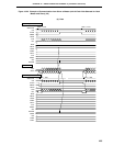
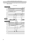
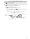
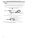
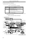
Preventive measure This restriction can be avoided by modifying the program.
Before executing the wake-up function, execute the following program that releases serial
transfer status. To execute the wake-up function, do not execute an instruction that
writes SIO0. Even if such an instruction is not executed, data can be received when the
wake-up function is executed.
This program releases the serial transfer status. To release the serial transfer status,
the serial interface channel 0 must be set once in the operation stop status (by clearing
the CSIE0 flag (bit 7 of the serial operation mode register (CSIM0) to 0). However, if the
serial interface channel 0 is set in the operation stop status in the I
2
C bus mode, the SCL
pin output a high level and the SDA0 (SDA1) pin outputs a low level, affecting
communication of the I
2
C bus. Therefore, this program places the SCL and SDA0 (SDA1)
pins in the high-impedance state to prevent the I
2
C bus from being affected.
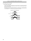
In the example below, SDA0 (/P25) is used as a serial data input/output pin. When
SDA1 (/P26) is used as the serial data input/output pin, take P2.5 and PM2.5 in the
program below as P2.6 and PM2.6, respectively
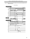
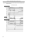
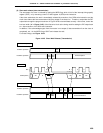
For the timing of each signal when this program is executed, refer to Figure 18-22.