


306
CHAPTER 15 A/D CONVERTER
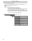
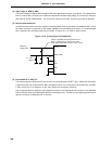
(2) Input range of ANI0 to ANI7
The input voltages of ANI0 to ANI7 should be within the specification range. In particular, if a voltage above
AV
REF0 or below AVSS is input (even if within the absolute maximum rating range), the conversion value for
that channel will be indeterminate. The conversion values of the other channels may also be affected.
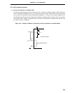
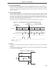
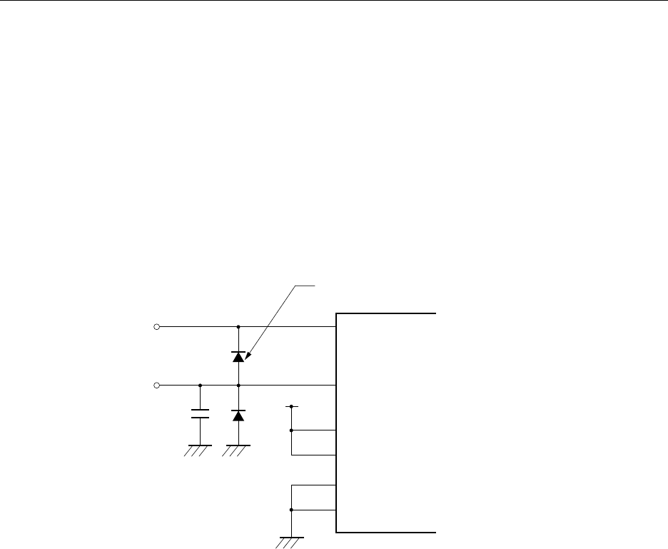
(3) Noise countermeasures
In order to maintain 8-bit resolution, attention must be paid to noise on pins AV
REF0 and ANI0 to ANI7. Since
the effect increases in proportion to the output impedance of the analog input source, it is recommended
that a capacitor be connected externally as shown in Figure 15-10 in order to reduce noise.
Figure 15-10. Analog Input Pin Disposition
(4) Pins ANI0/P10 to ANI7/P17
The analog input pins ANI0 to ANI7 also function as input/output port (PORT1) pins. When A/D conversion
is performed with any of pins ANI0 to ANI7 selected, be sure not to execute an input instruction to PORT
1 while conversion is in progress, as this may reduce the conversion resolution.
Also, if digital pulses are applied to a pin adjacent to the pin in the process of A/D conversion, the expected
A/D conversion value may not be obtainable due to coupling noise. Therefore, avoid applying pulses to pins
adjacent to the pin undergoing A/D conversion.
AV
REF0
or higher or AV
SS
or lower may enter,
ANI0 to ANI7
AV
REF0
V
DD
AV
DD
AV
SS
V
SS
Reference
Voltage Input
C = 100 to
1000 pF
If there is possibility that noise whose level is
clamp with a diode with a small V
F
(0.3 V or less).
V
DD