


375
CHAPTER 18 SERIAL INTERFACE CHANNEL 0 (
µ
PD78078Y Subseries)
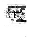
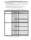
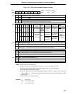
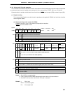
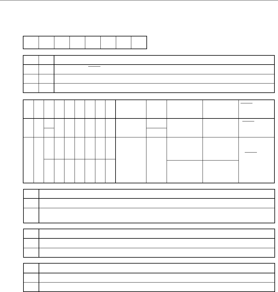
Figure 18-4. Serial Operating Mode Register 0 Format
Notes 1. Bit 6 (COI) is a read-only bit.
2. I
2
C bus mode, the clock frequency becomes 1/16 of that output from TO2.
3. Can be used as P25 (CMOS input/output) when used only for transmission.
4. Can be used freely as port function.
5. Set bit 5 (SIC) of the interrupt timing specify register (SINT) to 1 when using the wake-up
function (WUP = 1). Do not execute a write instruction to the serial I/O shift register 0 (SIO0)
while WUP = 1.
6. When CSIE0 = 0, COI becomes 0.
Remark x : Don’t care
PMxx : Port mode register
Pxx : Port output latch
<6><5>43210<7>Symbol
CSIM0 CSIE0 COI WUP
CSIM04 CSIM03 CSIM02 CSIM01 CSIM00
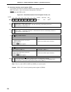
CSIM01
0
1
Serial Interface Channel 0 Clock Selection
Input clock to SCK0/SCL pin from off-chip
8-bit timer register 2 (TM2) output
0
R/W
1 Clock specified with bits 0 to 3 of timer clock select register 3 (TCL3)
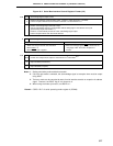
CSIM
04
0
CSIM00
x
0
1
FF60H 00H R/W
Note 1
Address After Reset R/W
R/W
CSIM
03
CSIM
02
PM25 P25 PM26 P26
PM27
P27
Operation
Mode
Start Bit
SI0/SB0/SDA0/
P25 Pin Function
SO0/SB1/SDA1/
P26 Pin Function
SCK0/SCL/P27
Pin Function
x
1
MSB
LSB
1x0001
Note 3
3-wire serial
l/O mode
SI0
(Input)
SO0
(CMOS output)
SCK0 (CMOS
input/output)
Note 3
2-wire serial
l/O mode
or
I
2
C bus mode
0
SCK0/SCL
(N-ch open-drain
input/output)
1
11
x
0
x
0
0
x
0
x
0
0
1
1
Note 4 Note 4
Note 4 Note 4
MSB
P25 (CMOS
input/output)
SB0/SDA0
(N-ch open-drain
input/output)
SB1/SDA1
(N-ch open-drain
input/output)
P26 (CMOS
input/output)
Note 3
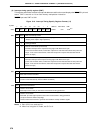
WUP
0
1
Wake-up Function Control
Note 5
Interrupt request signal generation with each serial transfer in any mode
Interrupt request signal generation when the address received after detecting start condition
(when CMDD = 1) matches the slave address register (SVA) data in I
2
C bus mode
R/W
COI
0
1
Slave Address Comparison Result Flag
Note 6
Slave address register (SVA) not equal to serial I/O shift register 0 (SIO0) data
Slave address register (SVA) equal to serial I/O shift register 0 (SIO0) data
R
CSIE0
0
1
Serial Interface Channel 0 Operation Control
Operation stopped
Operation enabled
R/W
Note 2