


419
CHAPTER 19 SERIAL INTERFACE CHANNEL 1
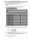
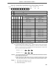
Notes 1. If the external clock input has been selected with CSIM11 set to 0, set bit 1 (BUSY1) and bit 2 (STRB)
of the automatic data transmit/receive control register (ADTC) to 0, 0.
2. Can be used freely as port function.
3. Can be used as P20 (CMOS input/output) when only transmitter is used (set bit 7 (RE) of ADTC to
0).
Remark x : Don’t care
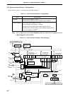
PMxx: Port mode register
Pxx : Port output latch
Operation
enable
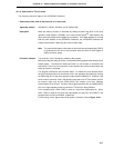
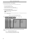
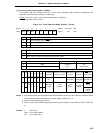
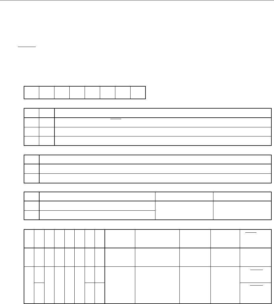
6<5>43210<7>Symbol
CSIM1 CSIE1 DIR ATE 0 0 0
CSIM11 CSIM10
CSIM11
0
1
Serial Interface Channel 1 Clock Selection
Clock externally input to SCK1 pin
Note 1
8-bit timer register 2 (TM2) output
SCK1
(Input)
1 Clock specified with bits 4 to 7 of timer clock select register 3 (TCL3)
CSIE
1
0
CSIM10
x
0
1
FF68H 00H R/W
Address After Reset R/W
CSIM
11
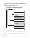
P20 PM21 P21 PM22
Shift Register
1 Operation
Serial Clock Counter
Operation Control
SI1/P20 Pin
Function
SCK1/P22
Pin Function
x
1
0
1
0
x00
1x
1
Note 2 Note 2
Note 2 Note 2
Count
operation
SI1
Note 3
(input)
xxxxx
Operation
stop
Clear P20 (CMOS
input/output)
P22 (CMOS
input/output)
ATE
0
1
Serial Interface Channel 1 Operating Mode Selection
3-wire serial I/O mode
3-wire serial I/O mode with automatic transmit/receive function
DIR
0
1
Start Bit
MSB
LSB
SI1 Pin Function
SI1/P20
(Input)
SO1 Pin Function
SO1
(CMOS output)
x
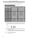
PM20
SO1/P21 Pin
Function
SO1 (CMOS
output)
P21 (CMOS
input/output)
SCK1
(CMOS
output)
1
Note 2
Note 2
Note 3Note 3
P22
(2) Serial operating mode register 1 (CSIM1)
This register sets serial interface channel 1 serial clock, operating mode, operation enable/stop, and
automatic transmit/receive operation enable/stop.
CSIM1 is set with a 1-bit or 8-bit memory manipulation instruction.
RESET input sets CSIM1 to 00H.
Figure 19-3. Serial Operation Mode Register 1 Format