


350
CHAPTER 17 SERIAL INTERFACE CHANNEL 0 (
µ
PD78078 SUBSERIES)
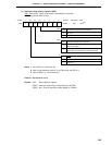
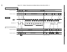
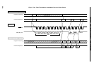
(5) Pin configuration
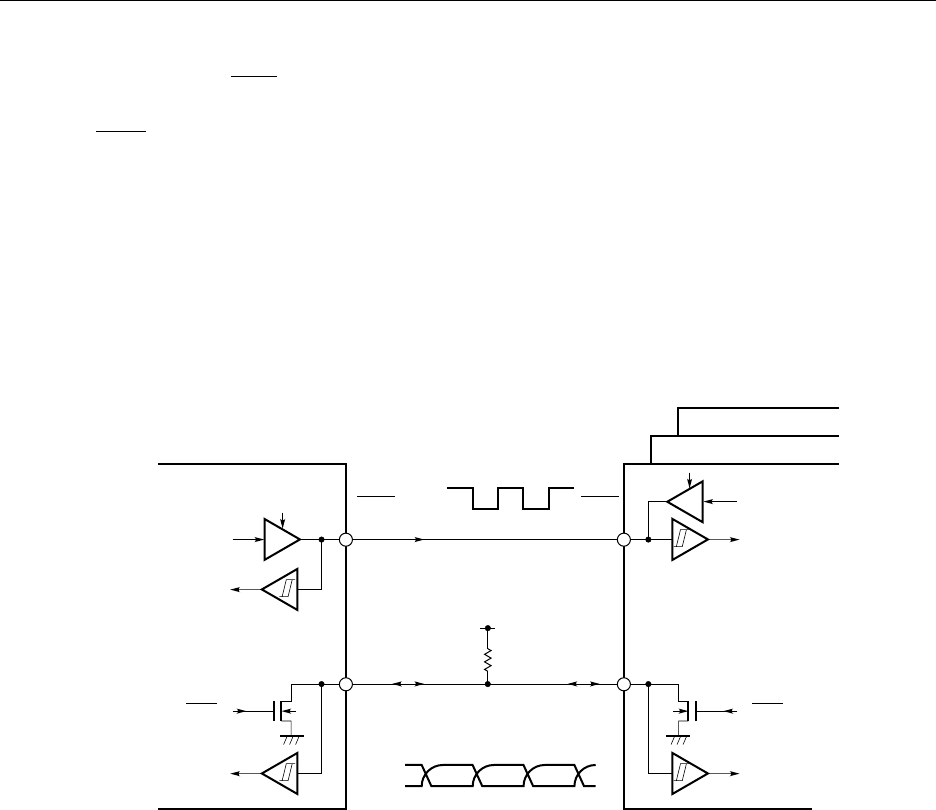
The serial clock pin SCK0 and serial data bus pin SB0 (SB1) have the following configurations.
(a) SCK0 ............ Serial clock input/output pin
<1> Master ... CMOS and push-pull output
<2> Slave ..... Schmitt input
(b) SB0 (SB1).... Serial data input/output dual-function pin
Both master and slave devices have an N-ch open drain output and a Schmitt input.
Because the serial data bus line has an N-ch open-drain output, an external pull-up resistor is necessary.
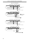
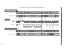
Figure 17-26. Pin Configuration
Caution Because the N-ch open-drain output must be high-impedance state at time of data
reception, write FFH to the serial I/O shift register 0 (SIO0) in advance. The N-ch open-drain
can be high-impedance state at any time of transfer. However, when the wake-up function
specify bit (WUP) = 1, the N-ch open-drain output is always high-impedance state. Thus,
it is not necessary to write FFH to SIO0.
SI0
SO0
SI0
SO0
(Clock Input)
Clock Output
Master Device
Clock Input
(Clock Output)
Serial Clock
SCK0
SCK0
R
L
Serial Data Bus
SB0 (SB1) SB0 (SB1)
N-ch Open Drain N-ch Open Drain
Slave Device