


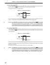
CHAPTER 17 SERIAL INTERFACE CHANNEL 0 (
µ
PD78078 SUBSERIES)
332
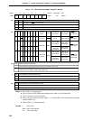
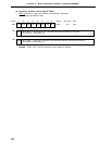
(4) MSB/LSB switching as the start bit
The 3-wire serial I/O mode enables to select transfer to start at MSB or LSB.
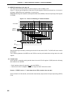
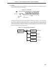
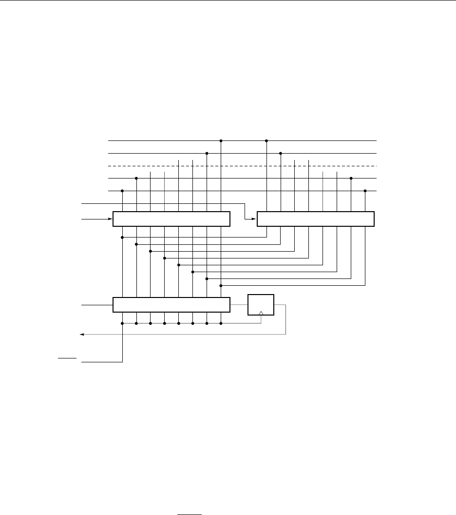
Figure 17-9 shows the configuration of the serial I/O shift register 0 (SIO0) and internal bus. As shown in
the figure, MSB/LSB can be read/written in reverse form.
MSB/LSB switching as the start bit can be specified with bit 2 (CSIM02) of the serial operating mode register
0 (CSIM0).
Figure 17-9. Circuit of Switching in Transfer Bit Order
Start bit switching is realized by switching the bit order for data write to SIO0. The SIO0 shift order remains
unchanged.
Thus, switching between the MSB-first and LSB-first must be performed before writing data to the shift
register.
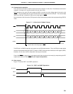
(5) Transfer start
Serial transfer is started by setting transfer data to the serial I/O shift register 0 (SIO0) when the following
two conditions are satisfied.
• Serial interface channel 0 operation control bit (CSIE0) = 1.
• Internal serial clock is stopped or SCK0 is a high level after 8-bit serial transfer.
Caution If CSIE0 is set to “1” after data write to SIO0, transfer does not start.
Upon termination of 8-bit transfer, serial transfer automatically stops and the interrupt request flag (CSIIF0)
is set.
7
6
Internal Bus
1
0
LSB-first
MSB-first Read/Write Gate
SI0 Shift Register 0 (SIO0)
Read/Write Gate
SO0
SCK0
DQ
SO0 Latch